STEVAL-ISA038V1 STMicroelectronics, STEVAL-ISA038V1 Datasheet - Page 5
STEVAL-ISA038V1
Manufacturer Part Number
STEVAL-ISA038V1
Description
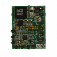
BOARD EVALUATION W/L6728
Manufacturer
STMicroelectronics
Type
DC/DC Switching Converters, Regulators & Controllersr
Specifications of STEVAL-ISA038V1
Design Resources
STEVAL-ISA038V1 Schematic STEVAL-ISA038V1 Bill of Material
Main Purpose
DC/DC, Step Down
Outputs And Type
1, Non-Isolated
Voltage - Output
1.25V
Current - Output
5A
Voltage - Input
5 ~ 12V
Regulator Topology
Buck
Frequency - Switching
300kHz
Board Type
Fully Populated
Utilized Ic / Part
L6728
Input Voltage
5 V to 12 V
Output Voltage
1.25 V
Product
Power Management Modules
Silicon Manufacturer
ST Micro
Silicon Core Number
L6728D
Kit Application Type
Power Management - Voltage Regulator
Application Sub Type
Step Down DC/DC Controller
Kit Contents
Board
Lead Free Status / RoHS Status
Lead free / RoHS Compliant
Power - Output
-
Lead Free Status / Rohs Status
Lead free / RoHS Compliant
For Use With/related Products
L6728
Other names
497-8228
STEVAL-ISA038V1
STEVAL-ISA038V1
Available stocks
Company
Part Number
Manufacturer
Quantity
Price
Company:

Part Number:
STEVAL-ISA038V1
Manufacturer:
STMicroelectronics
Quantity:
1


L6728
2
2.1
Pin description and connection diagrams
Pin descriptions
Table 2.
Figure 3.
Pin #
1
2
3
4
5
6
7
8
LGATE / OC
COMP / DIS
PHASE
UGATE
Pins description
Name
BOOT
Pin connection (top view)
GND
VCC
FB
HS driver supply.
Connect through a capacitor (100 nF) to the floating node (LS-Drain) pin
and provide necessary bootstrap diode from VCC.
HS driver return path, current-reading and adaptive-dead-time monitor.
Connect to the LS drain to sense
current. This pin is also used by the adaptive-dead-time control circuitry to
monitor when HS MOSFET is OFF.
HS driver output. Connect directly to HS MOSFET gate.
LGATE. LS driver output. Connect directly to LS MOSFET gate.
OC. Over Current threshold set. During a short period of time following
VCC rising over UVLO threshold, a 10 μA current is sourced from this pin.
Connect to GND with an R
Threshold. The resulting voltage at this pin is sampled and held internally
as the OC set point. Maximum programmable OC threshold is 0.55 V. A
voltage greater than 0.6 V activates an internal clamp and causes OC
threshold to be set at the maximum value.
All internal references, logic and drivers are connected to this pin.
Connect to the PCB ground plane.
Device and drivers power supply.
Operative range from 5 V to 12 V. Filter with at least 1 nF MLCC to GND.
COMP. Error amplifier output. Connect with an R
compensate the device control loop.
DIS. The device can be disabled by pushing this pin lower than 0.75 V (typ).
Setting free the pin, the device enables again.
Error amplifier inverting input.
Connect with a resistor R
divider may be used to regulate voltages higher than the reference.
FB
OCSET
Pin description and connection diagrams
to the output regulated voltage. Output resistor
Function
resistor greater than 5 kΩ to program OC
R
DS(on)
drop to measure the output
F
- C
F
// C
P
to FB to
5/31
Related parts for STEVAL-ISA038V1
Image
Part Number
Description
Manufacturer
Datasheet
Request
R

Part Number:
Description:
BOARD RGB CTR ST7,STP08C596MTR
Manufacturer:
STMicroelectronics
Datasheet:

Part Number:
Description:
Power Management IC Development Tools Full Speed USB to RS232 Bridge Demo
Manufacturer:
STMicroelectronics
Datasheet:
Part Number:
Description:
Power Management IC Development Tools 2.5W solar eval BRD USB SPV1040 LD39050
Manufacturer:
STMicroelectronics
Datasheet:

Part Number:
Description:
BOARD EVAL FOR MEMS SENSORS
Manufacturer:
STMicroelectronics
Datasheet:

Part Number:
Description:
KIT DEV STARTER ST10F276Z5
Manufacturer:
STMicroelectronics
Datasheet:

Part Number:
Description:
BOARD EVAL HDMI $ VIDEO SWITCH
Manufacturer:
STMicroelectronics
Datasheet:

Part Number:
Description:
BOARD DEMO ACCELEROMETER DIL24
Manufacturer:
STMicroelectronics
Datasheet:

Part Number:
Description:
BOARD STLM75/STDS75/ST72F651
Manufacturer:
STMicroelectronics
Datasheet:

Part Number:
Description:
EVAL BOARD 3AXIS MEMS ACCELLRMTR
Manufacturer:
STMicroelectronics
Datasheet:

Part Number:
Description:
BOARD EVAL 8BIT MICRO + TDE1708
Manufacturer:
STMicroelectronics
Datasheet:
Part Number:
Description:
STMicroelectronics [RIPPLE-CARRY BINARY COUNTER/DIVIDERS]
Manufacturer:
STMicroelectronics
Datasheet:
Part Number:
Description:
STMicroelectronics [LIQUID-CRYSTAL DISPLAY DRIVERS]
Manufacturer:
STMicroelectronics
Datasheet:
Part Number:
Description:
BOARD EVAL FOR MEMS SENSORS
Manufacturer:
STMicroelectronics
Datasheet: