CDB-43L21 Cirrus Logic Inc, CDB-43L21 Datasheet - Page 34
CDB-43L21
Manufacturer Part Number
CDB-43L21
Description
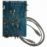
EVAL BOARD FOR CS43L21
Manufacturer
Cirrus Logic Inc
Specifications of CDB-43L21
Number Of Dac's
2
Number Of Bits
24
Outputs And Type
2, Single Ended
Sampling Rate (per Second)
96k
Data Interface
I²C, SPI™
Dac Type
Voltage
Voltage Supply Source
Analog and Digital
Operating Temperature
-10°C ~ 70°C
Utilized Ic / Part
CS43L21
Lead Free Status / RoHS Status
Lead free / RoHS Compliant
Other names
598-1282
CDB-43L21
CDB-43L21


34
SCL
SDA
SDA
SCL
START
ment bit in MAP allows successive reads or writes of consecutive registers. Each byte is separated by an
acknowledge bit. The ACK bit is output from the
CS43L21
Since the read operation cannot set the MAP, an aborted write operation is used as a preamble. As shown
in
dition. The following pseudocode illustrates an aborted write operation followed by a read operation.
Setting the auto-increment bit in the MAP allows successive reads or writes of consecutive registers. Each
byte is separated by an acknowledge bit.
START
Figure
0
1
CHIP ADDRESS (WRITE)
0
1
1
0
CHIP ADDRESS (WRITE)
Send start condition.
Send 100101x0 (chip address & write operation).
Receive acknowledge bit.
Send MAP byte, auto-increment off.
Receive acknowledge bit.
Send stop condition, aborting write.
Send start condition.
Send 100101x1 (chip address & read operation).
Receive acknowledge bit.
Receive byte, contents of selected register.
Send acknowledge bit.
Send stop condition.
0
2
1
0
from the microcontroller after each transmitted byte.
20, the write operation is aborted after the acknowledge for the MAP byte by sending a stop con-
1
3
0
2
0 1 AD0 0
4
1
3
5
0
4
6
1
5
7
AD0
ACK
6
8
7
9
INCR
0
ACK
10 11
Figure 20. Control Port Timing, I²C Read
Figure 19. Control Port Timing, I²C Write
8
6
INCR
9
5
MAP BYTE
12 13 14 15
10 11
4
6
MAP BYTE
3
5
2
12
4
1
13 14 15
3
16
0
ACK
2
STOP
17 18
START
1
16 17 18
CS43L21
0
19
ACK
1
20 21 22 23 24
CHIP ADDRESS (READ)
0
7
0
19
6
DATA
1
after each input byte is read and is input to the
0
24 25
1
1 AD0 1
0
25
ACK
26
26 27 28
27 28
ACK
7
DATA +1
6
7
DATA
0
1
ACK
0
DATA +1
7
7
DATA +n
0
6
DATA + n
1
7
CS43L21
0
0
ACK
ACK
NO
DS723A1
STOP
STOP
Related parts for CDB-43L21
Image
Part Number
Description
Manufacturer
Datasheet
Request
R

Part Number:
Description:
Development Kit
Manufacturer:
Cirrus Logic Inc
Datasheet:
Part Number:
Description:
Development Kit
Manufacturer:
Cirrus Logic Inc
Datasheet:


Part Number:
Description:
High-efficiency PFC + Fluorescent Lamp Driver Reference Design
Manufacturer:
Cirrus Logic Inc
Datasheet:
Part Number:
Description:
Development Kit
Manufacturer:
Cirrus Logic Inc
Datasheet:
Part Number:
Description:
Development Kit
Manufacturer:
Cirrus Logic Inc
Datasheet:

Part Number:
Description:
Development Kit
Manufacturer:
Cirrus Logic Inc
Datasheet:
Part Number:
Description:
Development Kit
Manufacturer:
Cirrus Logic Inc
Datasheet:
Part Number:
Description:
Development Kit
Manufacturer:
Cirrus Logic Inc
Datasheet:
Part Number:
Description:
Development Kit
Manufacturer:
Cirrus Logic Inc
Datasheet:

Part Number:
Description:
EVALUATION BOARD FOR CS8427
Manufacturer:
Cirrus Logic Inc
Datasheet:

Part Number:
Description:
BOARD EVAL FOR CS8416 RCVR
Manufacturer:
Cirrus Logic Inc
Datasheet:

Part Number:
Description:
EVALUATION BOARD FOR CS8420
Manufacturer:
Cirrus Logic Inc
Datasheet:

Part Number:
Description:
KIT DEVELOPMENT EP9315 ARM9
Manufacturer:
Cirrus Logic Inc
Datasheet:

Part Number:
Description:
KIT DEVELOPMENT EP9302 ARM9
Manufacturer:
Cirrus Logic Inc
Datasheet: