LM2794EVAL National Semiconductor, LM2794EVAL Datasheet - Page 3
LM2794EVAL
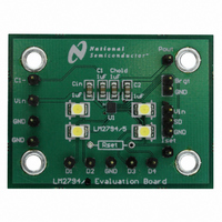
Manufacturer Part Number
LM2794EVAL
Description
BOARD EVALUATION LM2794
Manufacturer
National Semiconductor
Specifications of LM2794EVAL
Current - Output / Channel
80mA
Outputs And Type
4, Non-Isolated
Voltage - Output
4 V
Features
Charge Pump
Voltage - Input
2.7 ~ 5.5V
Utilized Ic / Part
LM2794
Lead Free Status / RoHS Status
Not applicable / Not applicable


I
V
I
I
I
I
I
I
V
V
V
V
I
R
I
DX
DX
DX
D-MATCH
Q
SD
PULL-SD
LEAK-SD
SET
DX
CP
CPH
IH
IL
BRGT
Absolute Maximum Ratings
If Military/Aerospace specified devices are required,
please contact the National Semiconductor Sales Office/
Distributors for availability and specifications.
Electrical Characteristics
Limits in standard typeface are for T
Range (−30˚C ≤ T
=124Ω ; LM2794:V
Symbol
V
SD
BRGT
Continuous Power Dissipation
(Note 2)
T
JMAX
IN
(Note 2)
Available Current at Output Dx
Available Voltage at Output Dx
Line Regulation of Dx Output
Current
Load Regulation of Dx Output
Current
Current Matching Between Any
Two Outputs
Quiescent Supply Current
Shutdown Supply Current
Shutdown Pull-Up Current
(LM2795)
Input Charge-Pump Mode To
Pass Mode Threshold
Input Charge-Pump Mode To
Pass Mode Hysteresis
SD Input Logic High (LM2794)
SD Input Logic High (LM2795)
SD Input Logic Low (LM2794)
SD Input Logic Low (LM2795)
SD Input Leakage Current
BRGT Input Resistance
I
SET
Pin Output Current
J
SD
≤ +100˚C). Unless otherwise specified, C1 = C2 = C
= V
Parameter
IN
(LM2795: V
J
−0.5 to (V
−0.5 to (V
= 25˚C and limits in boldface type apply over the full Operating Junction Temperature
SD
−0.5 to 6.2V max
Internally Limited
= 0V).
(Note 1)
IN
IN
3.0V ≤ V
V
BRGT = 50mV
2.7V ≤ V
V
BRGT = 0V
V
BRGT = 200mV
3.0V ≤ V
I
BRGT = 50mV
3.0V ≤ V
V
3.0V ≤ V
V
V
3.0V ≤ V
V
3.0V ≤ V
Load Current
R
3.0V ≤ V
V
(Note 5)
3.0V ≤ V
3.0V ≤ V
0V ≤ V
DX
+0.3V) w/
+0.3V) w/
6.2V max
6.2V max
DX
DX
DX
DX
DX
IN
IN
SET
IN
≤ 15mA
= 3.6V
= 3.6V, V
= 3.6V
135˚C
≤ 3.8V
≤ 3.6V
≤ 3.8V
= 3.6V
= 3.6V
= OPEN
SD
IN
IN
IN
IN
IN
DX
IN
IN
IN
IN
≤ V
Conditions
≤ 5.5V
≤ 3.0V
≤ 5.5V
≤ 5.5V
≤ 4.4V
≤ 4.2V, Active, No
≤ 5.5V, Shutdown
≤ 5.5V
≤ 5.5V
≤ 3.8V
DX
IN
3
= 3.6V
Operating Conditions
θ
Storge Temperature
Lead Temp. (Soldering, 5 sec.)
ESD Rating (Note 4)
Input Voltage (V
Ambient Temperature (T
Junction Temperature (T
JA
(Notes 2, 3)
Human Body Model
Machine Model
IN
= C
HOLD
IN
0.8V
= 1 µF, V
14.18
14.18
14.18
)
Min
3.8
1.0
15
10
20
IN
A
J
)
)
IN
I
15.25
15.25
15.25
= 3.6V, BRGT pin = 0V; R
DX
16.8
Typ
250
100
240
0.5
5.5
2.3
1.5
4.7
/10
0.2V
−65˚C to +150˚C
−30˚C to +100˚C
16.78
16.32
16.32
Max
−30˚C to +85˚C
8.2
0.2
5
2.7V to 5.5V
IN
www.national.com
125˚C/W
260˚C
200V
Units
2kV
mA
mA
mA
mA
mA
mA
mA
mV
mA
kΩ
µA
µA
nA
%
V
V
V
V
SET
Related parts for LM2794EVAL
Image
Part Number
Description
Manufacturer
Datasheet
Request
R

Part Number:
Description:
Accurate, 120 C-150 C Factory Preset Thermostat Lm27 Form
Manufacturer:
National Semiconductor Corporation
Datasheet:

Part Number:
Description:
Factory Preset Thermostat
Manufacturer:
National Semiconductor
Datasheet:
Part Number:
Description:
National Semiconductor [8-Bit D/A Converter]
Manufacturer:
National Semiconductor
Datasheet:
Part Number:
Description:
National Semiconductor [Media Coprocessor]
Manufacturer:
National Semiconductor
Datasheet:
Part Number:
Description:
Digitally Controlled Tone and Volume Circuit with Stereo Audio Power Amplifier, Microphone Preamp Stage and National 3D Sound
Manufacturer:
National Semiconductor
Datasheet:
Part Number:
Description:
Digitally Controlled Tone and Volume Circuit with Stereo Audio Power Amplifier, Microphone Preamp Stage and National 3D Sound
Manufacturer:
National Semiconductor
Datasheet:
Part Number:
Description:
AC97 Rev 2 Codec with Sample Rate Conversion and National 3D Sound
Manufacturer:
National Semiconductor
Part Number:
Description:
Manufacturer:
National Semiconductor
Datasheet:
Part Number:
Description:
Manufacturer:
National Semiconductor
Datasheet:
Part Number:
Description:
General Purpose, Low Voltage, Low Power, Rail-to-Rail Output Operational Amplifiers
Manufacturer:
National Semiconductor
Datasheet:
Part Number:
Description:
8-bit 20 MSPS flash A/D converter.
Manufacturer:
National Semiconductor
Datasheet:
Part Number:
Description:
Low Noise Quad Operational Amplifier
Manufacturer:
National Semiconductor
Datasheet:
Part Number:
Description:
Quad Differential Line Receivers
Manufacturer:
National Semiconductor
Datasheet:
Part Number:
Description:
Quad High Speed Trapezoidal? Bus Transceiver
Manufacturer:
National Semiconductor
Datasheet: