LM2794EVAL National Semiconductor, LM2794EVAL Datasheet - Page 4
LM2794EVAL
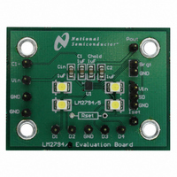
Manufacturer Part Number
LM2794EVAL
Description
BOARD EVALUATION LM2794
Manufacturer
National Semiconductor
Specifications of LM2794EVAL
Current - Output / Channel
80mA
Outputs And Type
4, Non-Isolated
Voltage - Output
4 V
Features
Charge Pump
Voltage - Input
2.7 ~ 5.5V
Utilized Ic / Part
LM2794
Lead Free Status / RoHS Status
Not applicable / Not applicable


www.national.com
f
SW
Electrical Characteristics
Limits in standard typeface are for T
Range (−30˚C ≤ T
=124Ω ; LM2794:V
Note 1: Absolute maximum ratings indicate limits beyond which damage to the device may occur. Electrical specifications do not apply when operating the device
beyond its rated operating conditions.
Note 2: Internal thermal shutdown circuitry protects the device from permanent damage. Thermal shutdown engages at T
T
Note 3: The value of θ
Note 4: In the test circuit, all capacitors are 1.0µF, 0.3Ω maximum ESR capacitors. Capacitors with higher ESR will increase output resistance, reduce output
voltage and efficiency.
Note 5: Voltage at which the device switches from charge-pump mode to pass mode or pass mode to charge-pump mode. For example, during pass mode the
device output (Pout) follows the input voltage.
Note 6: The output switches operate at one eigth of the oscillator frequency, f
Symbol
J
=140˚C (typ.). D1, D2, D3 and D4 may be shorted to GND without damage. P
Switching Frequency (Note 6)
JA
J
SD
≤ +100˚C). Unless otherwise specified, C1 = C2 = C
is based on a two layer evaluation board with a dimension of 2in. x1.5in.
= V
Parameter
IN
(LM2795: V
J
= 25˚C and limits in boldface type apply over the full Operating Junction Temperature
SD
= 0V).
(Continued)
3.0V ≤ V
IN
Conditions
≤ 4.4V
OSC
4
OUT
= 1/8f
may be shorted to GND for 1sec without damage.
SW
.
IN
= C
HOLD
= 1 µF, V
Min
325
IN
= 3.6V, BRGT pin = 0V; R
Typ
515
J
=150˚C (typ.) and disengages at
Max
675
Units
kHz
SET
Related parts for LM2794EVAL
Image
Part Number
Description
Manufacturer
Datasheet
Request
R

Part Number:
Description:
Accurate, 120 C-150 C Factory Preset Thermostat Lm27 Form
Manufacturer:
National Semiconductor Corporation
Datasheet:

Part Number:
Description:
Factory Preset Thermostat
Manufacturer:
National Semiconductor
Datasheet:
Part Number:
Description:
National Semiconductor [8-Bit D/A Converter]
Manufacturer:
National Semiconductor
Datasheet:
Part Number:
Description:
National Semiconductor [Media Coprocessor]
Manufacturer:
National Semiconductor
Datasheet:
Part Number:
Description:
Digitally Controlled Tone and Volume Circuit with Stereo Audio Power Amplifier, Microphone Preamp Stage and National 3D Sound
Manufacturer:
National Semiconductor
Datasheet:
Part Number:
Description:
Digitally Controlled Tone and Volume Circuit with Stereo Audio Power Amplifier, Microphone Preamp Stage and National 3D Sound
Manufacturer:
National Semiconductor
Datasheet:
Part Number:
Description:
AC97 Rev 2 Codec with Sample Rate Conversion and National 3D Sound
Manufacturer:
National Semiconductor
Part Number:
Description:
Manufacturer:
National Semiconductor
Datasheet:
Part Number:
Description:
Manufacturer:
National Semiconductor
Datasheet:
Part Number:
Description:
General Purpose, Low Voltage, Low Power, Rail-to-Rail Output Operational Amplifiers
Manufacturer:
National Semiconductor
Datasheet:
Part Number:
Description:
8-bit 20 MSPS flash A/D converter.
Manufacturer:
National Semiconductor
Datasheet:
Part Number:
Description:
Low Noise Quad Operational Amplifier
Manufacturer:
National Semiconductor
Datasheet:
Part Number:
Description:
Quad Differential Line Receivers
Manufacturer:
National Semiconductor
Datasheet:
Part Number:
Description:
Quad High Speed Trapezoidal? Bus Transceiver
Manufacturer:
National Semiconductor
Datasheet: