AS5040 DB V2 austriamicrosystems, AS5040 DB V2 Datasheet - Page 4
AS5040 DB V2
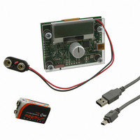
Manufacturer Part Number
AS5040 DB V2
Description
BOARD DEMO AS5040
Manufacturer
austriamicrosystems
Specifications of AS5040 DB V2
Sensor Type
Magnetic, Rotary Position
Sensing Range
360°
Interface
USB
Voltage - Supply
5V USB or 9V
Embedded
Yes, MCU, 8-Bit
Utilized Ic / Part
AS5040
Lead Free Status / RoHS Status
Lead free by exemption / RoHS compliant by exemption
Sensitivity
-


AS5040
Data Sheet
Pin 12 allows a single wire output of the 10-bit absolute position value. The value is encoded into a pulse width
modulated signal with 1µs pulse width per step (1µs to 1024µs over a full turn). By using an external low pass filter,
the digital PWM signal is converted into an analog voltage, allowing a direct replacement of potentiometers.
5 Electrical Characteristics
Absolute Maximum Ratings (non operating)
Stresses beyond those listed under “Absolute Maximum Ratings“ may cause permanent damage to the device. These are stress
ratings only. Functional operation of the device at these or any other conditions beyond those indicated under “Operating
Conditions” is not implied. Exposure to absolute maximum rating conditions for extended periods may affect device reliability.
Operating Conditions
DC Characteristics for Digital Inputs and Outputs
CMOS Schmitt-Trigger Inputs: CLK, CSn (CSn = internal Pull-up)
(operating conditions: T
unless otherwise noted)
www.austriamicrosystems.com
DC supply voltage at pin VDD5V
DC supply voltage at pin VDD3V3
Input pin voltage
Input current (latchup immunity)
Electrostatic discharge
Storage temperature
Body temperature (Lead-free
package)
Humidity non-condensing
Ambient temperature
Supply current
External supply voltage at pin VDD5V
Internal regulator output voltage at pin
VDD3V3
External supply voltage at pin VDD5V,
VDD3V3
High level input voltage
Low level input voltage
Schmitt Trigger hysteresis
Input leakage current
Pull-up low level input current
Parameter
Parameter
Parameter
amb
= -40 to +125°C, VDD5V = 3.0-3.6V (3V operation) VDD5V = 4.5-5.5V (5V operation)
VDD3V3
Symbol
VDD5V
TBody
Tstrg
Symbol
V
ESD
Iscr
Vin
Ion-
H
I
LEAK
V
V
I
VDD3V3
VDD3V3
iL
Symbol
IH
IL
VDD5V
VDD5V
V
T
I
Ioff
supp
amb
-100
Min
-0.3
-0.3
-0.3
-0.3
-55
5
0.7 * VDD5V
Min
-40
4.5
3.0
3.0
3.0
Min
Revision 2.10
-30
-1
1
VDD5V +0.3
Typ Max Unit
5.0
3.3
3.3
3.3
16
Max
100
125
260
7.5
± 2
85
7
5
125
5.5
3.6
3.6
3.6
21
0.3 * VDD5V
Max
-100
mA
Unit
°C
1
mA
V
V
V
V
kV
°C
°C
%
V
V
V
-40°F…+257°F
5V operation
3.3V operation (pins VDD5V and
VDD3V3 connected)
Pins MagIncn, MagDecn, CLK, CSn,
Pin Prog
Norm: JEDEC 78
Norm: MIL 883 E method 3015
Min – 67°F ; Max +257°F
t=20 to 40s, Norm: IPC/JEDEC J-
Std-020C
Lead finish 100% Sn “matte tin”
Unit
µA
µA
V
V
V
Normal operation
CLK only
CSn only, VDD5V: 5.0V
Note
Note
Note
4 - 33
Related parts for AS5040 DB V2
Image
Part Number
Description
Manufacturer
Datasheet
Request
R

Part Number:
Description:
IC ENCODER PROG 10-BIT 16-SSOP
Manufacturer:
austriamicrosystems
Datasheet:

Part Number:
Description:
BOARD ADAPTER AS5040
Manufacturer:
austriamicrosystems
Datasheet:

Part Number:
Description:
BOARD PROGRAM AS5040
Manufacturer:
austriamicrosystems
Datasheet:
Part Number:
Description:
IC ENCODER PROG 10-BIT 16-SSOP
Manufacturer:
austriamicrosystems
Datasheet:
Part Number:
Description:
10-bit Programmable Magnetic Rotary Encoder
Manufacturer:
austriamicrosystems
Datasheet:
Part Number:
Description:
IC SWITCH QUAD SPST 14-TSSOP
Manufacturer:
austriamicrosystems
Datasheet:
Part Number:
Description:
IC SWITCH QUAD SPST 14-TSSOP
Manufacturer:
austriamicrosystems
Datasheet:
Part Number:
Description:
IC AMP AUDIO MONO 1.8W 10-MSOP
Manufacturer:
austriamicrosystems
Datasheet:
Part Number:
Description:
IC AMP AUDIO MONO 1.8W 10-MSOP
Manufacturer:
austriamicrosystems
Datasheet:
Part Number:
Description:
IC AMP AUDIO MONO 1.8W 10-MSOP
Manufacturer:
austriamicrosystems
Datasheet:
Part Number:
Description:
IC AMP AUD 1.8W 3DB GAIN 10-MSOP
Manufacturer:
austriamicrosystems
Datasheet:
Part Number:
Description:
IC DRIVER LED 8-DIGIT 24-SOIC
Manufacturer:
austriamicrosystems
Datasheet:
Part Number:
Description:
IC DRIVER LED 8-DIGIT 24-SOIC
Manufacturer:
austriamicrosystems
Datasheet:
Part Number:
Description:
IC, LINE/SPEAKER PHONE CIRCUIT, SOIC-28
Manufacturer:
austriamicrosystems
Datasheet:
Part Number:
Description:
IC MULTI-STANDARD CMOS TELEPHONE SOIC-28
Manufacturer:
austriamicrosystems
Datasheet: