STEVAL-MKI064V1 STMicroelectronics, STEVAL-MKI064V1 Datasheet - Page 25
STEVAL-MKI064V1
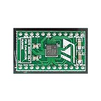
Manufacturer Part Number
STEVAL-MKI064V1
Description
BOARD ADAPTER LSM303DLH DIL24
Manufacturer
STMicroelectronics
Series
MEMSr
Datasheets
1.STEVAL-MKI009V1.pdf
(42 pages)
2.STEVAL-MKI063V1.pdf
(47 pages)
3.STEVAL-MKI064V1.pdf
(4 pages)
Specifications of STEVAL-MKI064V1
Sensor Type
Accelerometer and Magnetometer
Sensing Range
±2g, 4g, 8g, ±1.3 ~ 8.1 gauss
Interface
I²C
Sensitivity
1 ~ 3.9 mg/Digit, ±0.01%/°C
Embedded
No
Utilized Ic / Part
LSM303DLH
Sensing Axis
Double Axis
Output Type
Digital
Interface Type
USB
For Use With
497-10682 - MOTEHRBOARD MEMS ADAPTER STM32
Lead Free Status / RoHS Status
Lead free / RoHS Compliant
Voltage - Supply
-
Lead Free Status / Rohs Status
Lead free / RoHS Compliant
For Use With/related Products
LPR5xxxAL, LPY5xxxAL, LY5xxxAL
Other names
497-10689


LSM303DLH
7.1.2
Table 15.
7.1.3
Master
Slave
Linear acceleration digital interface
For linear acceleration, the default (factory) 7-bit slave address is 001100xb. The
SDO/SA0 pad can be used to modify the least significant bit of the device address. If the
SA0 pad is connected to voltage supply, LSb is ‘1’ (address 0011001b) otherwise if the SA0
pad is connected to ground, LSb value is ‘0’ (address 0011000b). This solution permits
connecting and addressing two different accelerometers to the same I
The slave address is completed with a read/write bit. If the bit was ‘1’ (read), a repeated
START (SR) condition will have to be issued after the two sub-address bytes; if the bit is ‘0’
(write) the master transmits to the slave with direction unchanged.
the SAD+Read/Write bit pattern is composed, listing all the possible configurations.
Table 14.
In order to read multiple bytes, it is necessary to assert the most significant bit of the sub-
address field. In other words, SUB(7) must be equal to 1 while SUB(6-0) represents the
address of the first register to be read.
In the presented communication format , MAK is Master Acknowledge and NMAK is No
Master Acknowledge.
Transfer when master is receiving (reading) multiple bytes of data from slave
Magnetic field digital interface
The system communicates via a two-wire I
protocol is defined by the I
kbps or 400 kbps rates as defined by the I
bit data/address send and a 1-bit acknowledge bit. The format of the data bytes (payload)
shall be case-sensitive ASCII characters or binary data to the magnetic sensor slave, and
binary data returned. Negative binary values will be in two’s complement form.
For magnetic sensor, the default (factory) 7-bit slave address is 0011110b
(0x3C) for write operations, or 00111101b (0x3D) for read operations.
The Serial Clock (SCL_M) and Serial Data (SDA_M) lines have optional internal pull-up
resistors, but require resistive pull-up (Rp) between the master device (usually a host
microprocessor) and the LSM303DLH. Pull-up resistance values of about 10 kΩ are
recommended with a nominal 1.8 V digital supply voltage (Vdd_dig_M).
ST
Command
SAD
+W
Read
Write
Read
Write
SAK
SAD+Read/Write patterns
SUB
SAD[6:1]
SAK
001100
001100
001100
001100
2
C bus specification. The data rate is the standard mode 100
SR
Doc ID 16941 Rev 1
SAD
+R
SAD[0] = SA0
SAK DATA
2
2
C bus specifications. The bus bit format is an 8-
C bus system as a slave device. The interface
0
0
1
1
MAK
DATA
R/W
1
0
1
0
Table 14
MAK
2
C lines.
Digital interfaces
DATA
00110001 (31h)
00110000 (30h)
00110011 (33h)
00110010 (32h)
explains how
SAD+R/W
NMAK SP
25/47
Related parts for STEVAL-MKI064V1
Image
Part Number
Description
Manufacturer
Datasheet
Request
R

Part Number:
Description:
BOARD EVAL FOR MEMS SENSORS
Manufacturer:
STMicroelectronics
Datasheet:

Part Number:
Description:
EVALBOARD/STEVAL-ISV014V1
Manufacturer:
STMicroelectronics
Part Number:
Description:
BOARD EVAL FOR ST802RT1
Manufacturer:
STMicroelectronics
Datasheet:

Part Number:
Description:
BOARD EVAL FOR VACUUM CLEANER
Manufacturer:
STMicroelectronics
Datasheet:

Part Number:
Description:
KIT DEV STARTER ST10F276Z5
Manufacturer:
STMicroelectronics
Datasheet:

Part Number:
Description:
BOARD LED CTLR/DVR STLED316S
Manufacturer:
STMicroelectronics
Datasheet:

Part Number:
Description:
BOARD EVAL BLDC SENSORLESS MOTOR
Manufacturer:
STMicroelectronics
Datasheet:

Part Number:
Description:
BOARD ELECT FISCAL CASH REGISTER
Manufacturer:
STMicroelectronics
Datasheet:

Part Number:
Description:
BOARD EVAL BIPO SOLUTION FOR PFC
Manufacturer:
STMicroelectronics
Datasheet:

Part Number:
Description:
BOARD EVAL UPS 450W VOUT=220V
Manufacturer:
STMicroelectronics
Datasheet:
Part Number:
Description:
STMicroelectronics [RIPPLE-CARRY BINARY COUNTER/DIVIDERS]
Manufacturer:
STMicroelectronics
Datasheet:
Part Number:
Description:
STMicroelectronics [LIQUID-CRYSTAL DISPLAY DRIVERS]
Manufacturer:
STMicroelectronics
Datasheet:
Part Number:
Description:
BOARD EVAL FOR MEMS SENSORS
Manufacturer:
STMicroelectronics
Datasheet: