DK-MAXII-1270N Altera, DK-MAXII-1270N Datasheet
DK-MAXII-1270N
Specifications of DK-MAXII-1270N
Available stocks


Related parts for DK-MAXII-1270N


DK-MAXII-1270N Summary of contents
Page 1
... Innovation Drive San Jose, CA 95134 (408) 544-7000 www.altera.com P25-10351-01 MAX II Development Kit Getting Started User Guide Development Kit Version: 1.1.0 Document Version: 1.1.0 Document Date: July 2005 ...
Page 2
... Altera Corporation in the U.S. and other countries. All other product or service names are the property of their respective holders. Al- tera products are protected under numerous U ...
Page 3
... About This User Guide Revision History ........................................................................................................................................ v How to Contact Altera .............................................................................................................................. v Typographic Conventions ...................................................................................................................... vi Chapter 1. About This Kit Features ................................................................................................................................................... 1–1 Chapter 2. Getting Started System Requirements ............................................................................................................................ 2–1 MAX II Development Kit Contents ............................................................................................... 2–1 Inspect the Board ............................................................................................................................. 2–1 Software Requirements ................................................................................................................... 2–1 Important Considerations ............................................................................................................... 2–2 Installing the MegaCore Function & Reference Designs/Demos .................................................. 2–2 Installing the Quartus II Software ....................................................................................................... 2– ...
Page 4
... Contents iv MAX II Development Kit Getting Started User Guide Development Kit Version 1.1.0 Altera Corporation July 2005 ...
Page 5
... How to Contact For technical support or other information about Altera the Altera world-wide web site at www.altera.com. You can also contact Altera Altera through your local sales representative or any of the sources listed below. Information Type Technical support www.altera.com/mysupport/ 800-800-EPLD (3753) 7:00 a ...
Page 6
... MAX II Development Kit Getting Started User Guide Meaning , \qdesigns directory, d: drive, chiptrip.gdf file. MAX , PIA , input. Active-low signals are denoted by suffix c:\qdesigns\tutorial\chiptrip.gdf ), as well as logic function names (e.g., SUBDESIGN Development Kit Version 1.1.0 , data1 n , e.g., resetn . . Also, sections are shown in TRI Altera Corporation July 2005 ...
Page 7
... SOPC design. The Quartus II software integrates into nearly any design environment, with interfaces to industry-standard EDA tools. You can obtain a 4-month license for the software from the Altera web site. The Quartus II license allows you to use the product for four months only. After four months, you must get a renewal to keep on using the software. ® ...
Page 8
... Features ■ 1–2 MAX II Development Kit Getting Started User Guide Reference Designs/Demos—Altera provides several demos and reference designs with the MAX II Development Kit to help you get started building applications. See “Reference Designs” on page 2–16 designs provided. Development Kit Version 1.1.0 “ ...
Page 9
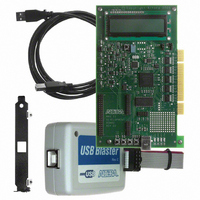
... Before using the kit or installing the software, be sure to check the contents of the kit and inspect the board to verify that you received all of Requirements the items. If any of these items are missing, contact Altera proceed. You should also verify that your PC meets the software and system requirements of the kit. ...
Page 10
... Reference Designs/Demos Figure 2–1 2–2 MAX II Development Kit Getting Started User Guide Altera recommends that you install the software that is on the MAX II Development Kit CD-ROM. See Function & Reference Designs/Demos”. Quartus II software version 4.1 SP1 or later. See Quartus II Software”. ...
Page 11
... Before using the Quartus II software, you must request a license file from the Altera web site at www.altera.com/licensing and install it on your Licensing PC. When you request a license file, Altera e-mails you a license.dat file that enables the software. To obtain a license, perform the following steps: 1. ...
Page 12
... To install your license, refer to “Specifying the License File” in the Quartus II Installation & Licensing Manual for PCs, included on the MAX II Development Kit CD-ROM. Align the ByteBlaster II connector so that the red strip is orientated towards the Altera logo on the board. for details regarding programming Development Kit Version 1.1.0 2–16. ...
Page 13
... Altera Corporation July 2005 Make sure the shunt on jumper J8 is connected to pins 1 and 2 (the two pins closest to the LCD on the board). This supplies power from the USB cable to the board power plane. Connect the USB cable from the USB port on your PC to the USB Type B connector on the MAX II development board ...
Page 14
... Program the board with FunctionalTest.pof, located in the <root>/Examples/HW/Demos directory. (Refer to the MAX II Device” on page 2–4 into the MAX II device.) The LCD should read “MAX II by Altera”. Push S2 to cycle through the tests. a. After pressing S2 once, the LCD screen should display the voltage of V ...
Page 15
... If all tests pass, the MAX II development board is ready to use. Altera provides several demos and reference designs with the MAX II Development Kit to help you get started building applications and to demonstrate the features of the MAX II device. The next two sections describe the functionality of these designs. ...
Page 16
... The power regulator can be set adding = 3.3 V.) The load on the regulator can be CCINT , V , GND, and a MAX II User I/O pin. These four CCINT CCIO Development Kit Version 1.1.0 supply to 2 3.3 V, CCINT is CCINT value is 3.3 V. CCINT level is reached MAX 2 the CCINT Altera Corporation July 2005 ...
Page 17
... Using the Demo Test 1: Race Against the MAX II Device Altera Corporation July 2005 Program the MAX II device with the InstantOn.pof demo, located in the <root>/Examples/HW/Demos directory. (Refer to “Programming the MAX II Device” on page 2–4 to load POF files into the MAX II device.) The following message scrolls across the LCD ...
Page 18
... GND = Board Ground plane ACTIVE_IO = MAX II User I/O pin P12 Development Kit Version 1.1.0 for details on how CCINT CC rise time CC and the resulting configuration CCINT can be varied with POT1, thus CCINT supply any time it is CCINT Altera Corporation July 2005 rise ...
Page 19
... Memory (CFM) to the configuration SRAM. The first falling edge on this I/O (shown in the lighter color in complete. Measuring back the T Active I/O will show at approximately what core voltage configuration started. Altera Corporation July 2005 rise time, and the rise time variation caused CC shows a typical digital oscilloscope output. For this test the rise time ...
Page 20
... Use Ohm’s Law to calculate the current and 2–12 MAX II Development Kit Getting Started User Guide (if the shunt place, CCINT = 2 the shunt is off, V CCINT Development Kit Version 1.1.0 and MAX I/O During Power-Up CCINT as the number of CCINT = 3.3 V). Note that the power can CCINT Altera Corporation July 2005 ...
Page 21
... The switches control the operation of this demo: ■ ■ ■ ■ Altera Corporation July 2005 This circuit uses resistors with a specified variance of 5%, which means that the power measurement is not precise. This circuit is provided to give users a general understanding of the MAX II device power consumption. Users who need a precise power ...
Page 22
... Open the VendingMachineDemo.pof file in the Quartus II software. Choose Options (Tools menu) and then click Programmer in the list of options on the left. Check the Enable real-time ISP to allow background programming check box. See Figure Development Kit Version 1.1.0 for details on “Running the 2–5. Altera Corporation July 2005 ...
Page 23
... Figure 2–5. Programmer Options Dialog Box Altera Corporation July 2005 Program the MAX II device with the VendingMachineDemo.pof file. Observe the Functional Test design still functioning as in step 2. Press S5, which interrupts the V and forces the MAX II device to reconfigure. Observe the Vending Machine Demo functioning as described below ...
Page 24
... This design was built such that both the software and hardware portions would be easy to understand, not for optimum speed or efficiency. 2–16 MAX II Development Kit Getting Started User Guide Development Kit Version 1.1.0 Altera Corporation July 2005 ...
Page 25
... Using the USB Reference Design Altera Corporation July 2005 Program the board with the USBReferenceDesign.pof file. (Refer to “Programming the MAX II Device” on page 2–4 to load POF files into the MAX II device.) To install the drivers, perform the following steps: a. When you plug the board into your PC, the message “Found New Hardware” ...
Page 26
... Found MAX II Board on port X (where X is the number of the port was unsuccessful, the status box reports Could not find MAX II Board. Development Kit Version 1.1.0 Figure 2–7 the Figure 2–6). Click Altera Corporation July 2005 ...
Page 27
... Figure 2–7. Device Manager Window 5. 6. Altera Corporation July 2005 If successful communication is established, the LCD displays Connected to PC!. The PC Application allows you to read from and write to most of the components on the MAX II board. Note the Default Encoding drop down box in the Control Options section of the user interface. ...
Page 28
... USB_Utility.exe file resides. This file is re-created each time you read from the SRAM. It contains the addresses and the data read from those addresses. 1 SRAMDataBack.txt must not be open when you try to read from the SRAM. Development Kit Version 1.1.0 Altera Corporation July 2005 ...
Page 29
... Temperature blocks. If data is received from the PC, then the Director passes control to the UFMInterface.v, the SRAMInterface.v, or the LCDInterface.v, depending on the value of the data received. Refer to the Verilog code itself for more details on the operation of this MAX II design. Altera Corporation July 2005 e. Read the UFM—The UFM is arranged as 256 locations, each containing 32 bits of data ...
Page 30
... The object of the game is to build a total bankroll of $1000 or more by using three levels of wagering. The game is initiated by hitting the Bet button (S2), at which time the player is given a default total of $199. By 2–22 MAX II Development Kit Getting Started User Guide Development Kit Version 1.1.0 Altera Corporation July 2005 ...
Page 31
... An LCD controller interprets the instructions provided by either path and supplies stimulus to the LCD hardware to render the appropriate images. See Altera Corporation July 2005 2–1. Play continues in this way until the player either reaches $1000 Wager ...
Page 32
... This block manages the status and functionality of the player controlled inputs Bet and Spin. The functionality of this block can be divided into three major areas: 2–24 MAX II Development Kit Getting Started User Guide Development Kit Version 1.1.0 Figure 2–9. Altera Corporation July 2005 ...
Page 33
... Based on the value of the 11-bit input bus, the controller handles changes to the speed, content, and direction (read/write) of LCD data. Altera Corporation July 2005 Start-up—When the MAX II device has been successfully programmed, the Control block automatically accesses a section of the UFM that prompts an introduction sequence to appear on the LCD screen ...
Page 34
... The PCI Reference Design provides an example of how users can interface the MAX II development board via the PCI expansion slots. The design uses Altera’s PCI T32 MegaCore function to interface to the PCI Bus of any standard PC. All design files are provided in the <root>/HW/Examples/ReferenceDesigns/PCI_Reference Design/QuartusProject/DesignFiles directory ...
Page 35
... Type the following commands: wdreg.exe -inf <root>\Examples\HW\ReferenceDesigns\ PCI_ReferenceDesign\Win2k_XP_Drivers\windrvr6.inf install r wdreg -inf <root>\Examples\HW\ReferenceDesigns\ PCI_ReferenceDesign\Win2k_XP_Drivers\ altera_maxiipci.inf install r Turn off your PC and install the MAX II development board in an available PCI slot. (Refer to your PC's hardware installation documentation.) Power-up the PC. Install the drivers: ...
Page 36
... The data read from the sensor is displayed in Centigrade. b. Click the F radio button to convert the value to Fahrenheit. following: v Click on the Read button (under the Config register group) of the application. The value of the various configuration registers is displayed in the application. Development Kit Version 1.1.0 Altera Corporation July 2005 ...
Page 37
... Push one of the four user-defined push switches on the board to Figure 2–10. Interrupt Received Dialog Box Altera Corporation July 2005 generate an interrupt. The application reads the corresponding register to figure out which switch was pushed and clears the interrupt. A dialog box appears when an interrupt is received (see Figure 2– ...
Page 38
... Reference Designs 2–30 MAX II Development Kit Getting Started User Guide Development Kit Version 1.1.0 Altera Corporation July 2005 ...