DK-MAXII-1270N Altera, DK-MAXII-1270N Datasheet - Page 29
DK-MAXII-1270N
Manufacturer Part Number
DK-MAXII-1270N
Description
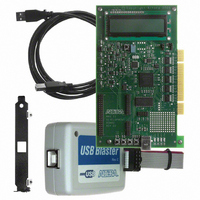
KIT DEV MAXII W/EPM 1270N
Manufacturer
Altera
Series
MAX® IIr
Type
CPLDr
Specifications of DK-MAXII-1270N
Contents
Dev Board, Quartus®II Web Edition, Nios®II Web Edition, Cables, Accessories, Reference Designs and Demos
Silicon Manufacturer
Altera
Core Architecture
CPLD
Core Sub-architecture
MAX
Silicon Core Number
EPM
Silicon Family Name
MAX II
Rohs Compliant
Yes
For Use With/related Products
MAX®II CPLDs
Lead Free Status / RoHS Status
Lead free / RoHS Compliant
Other names
544-2380
Available stocks
Company
Part Number
Manufacturer
Quantity
Price


Altera Corporation
July 2005
1
Understanding the Functionality of the USB Reference Design
The USB Reference Design has two pieces:
■
■
The MAX II design consists entirely of state machines. Each individual
design file contains a state machine to control the reading/writing of each
component. These files contain extensive comments and designers are
encouraged to look through the Verilog code to gain a complete
understanding of how the MAX II design functions. The Director.v code
constantly awaits for one of two things to happen: either a button is
pressed or data arrives from the PC. If a button is pressed, the Director
enables the PassivesInterface.v, which takes over control of the output to
the USB MAC FIFO and writes the values of the Switch Counters and
Temperature blocks. If data is received from the PC, then the Director
passes control to the UFMInterface.v, the SRAMInterface.v, or the
LCDInterface.v, depending on the value of the data received. Refer to the
Verilog code itself for more details on the operation of this MAX II design.
e.
1
f.
Verilog code written to dictate the functionality of the MAX II device
Visual Basic code to control the PC application
Development Kit Version 1.1.0
Read the UFM—The UFM is arranged as 256 locations, each
containing 32 bits of data. Currently residing in the UFM is the
inverse of each address. Set the default encoding to
Hexadecimal and click Read UFM. The data displayed should
be FFFF FFFE FFFD FFFC FFFB and so forth. You can recompile
this design with a different memory initialization file (MIF) to
change the data in the UFM. Note that when you read from the
UFM, a file called UFMDataBack.txt is created in the same
directory where the USB_Utility.exe file resides. This file is
re-created each time you read the UFM. It contains the
addresses and the data read from those addresses.
Display the board temperature and push button counts—Press the
S2, S3, and S4 buttons on the board. Note that each time a
button is pressed, the corresponding text box on the GUI
increments. Also note that the board temperature is updated
each time a switch is pressed.
The SRAM and UFM read/write options only read or write
384 bytes at a time. This data is always written to or read from
the 384 lowest address locations.
UFMDataBack.txt must not be open when you read from
the UFM.
MAX II Development Kit Getting Started User Guide
Getting Started
2–21
Related parts for DK-MAXII-1270N
Image
Part Number
Description
Manufacturer
Datasheet
Request
R

Part Number:
Description:
KIT DEV MAX V 5M570Z
Manufacturer:
Altera
Datasheet:

Part Number:
Description:
CYCLONE II STARTER KIT EP2C20N
Manufacturer:
Altera
Datasheet:


Part Number:
Description:
CPLD, EP610 Family, ECMOS Process, 300 Gates, 16 Macro Cells, 16 Reg., 16 User I/Os, 5V Supply, 35 Speed Grade, 24DIP
Manufacturer:
Altera Corporation
Datasheet:
Part Number:
Description:
CPLD, EP610 Family, ECMOS Process, 300 Gates, 16 Macro Cells, 16 Reg., 16 User I/Os, 5V Supply, 15 Speed Grade, 24DIP
Manufacturer:
Altera Corporation
Datasheet:
Part Number:
Description:
Manufacturer:
Altera Corporation
Datasheet:
Part Number:
Description:
CPLD, EP610 Family, ECMOS Process, 300 Gates, 16 Macro Cells, 16 Reg., 16 User I/Os, 5V Supply, 30 Speed Grade, 24DIP
Manufacturer:
Altera Corporation
Datasheet:
Part Number:
Description:
High-performance, low-power erasable programmable logic devices with 8 macrocells, 10ns
Manufacturer:
Altera Corporation
Datasheet:
Part Number:
Description:
High-performance, low-power erasable programmable logic devices with 8 macrocells, 7ns
Manufacturer:
Altera Corporation
Datasheet:
Part Number:
Description:
Classic EPLD
Manufacturer:
Altera Corporation
Datasheet:
Part Number:
Description:
High-performance, low-power erasable programmable logic devices with 8 macrocells, 10ns
Manufacturer:
Altera Corporation
Datasheet:
Part Number:
Description:
Manufacturer:
Altera Corporation
Datasheet:
Part Number:
Description:
Manufacturer:
Altera Corporation
Datasheet:
Part Number:
Description:
Manufacturer:
Altera Corporation
Datasheet: