DK-MAXII-1270N Altera, DK-MAXII-1270N Datasheet
DK-MAXII-1270N
Specifications of DK-MAXII-1270N
Available stocks


Related parts for DK-MAXII-1270N


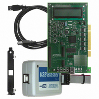
DK-MAXII-1270N Summary of contents
Page 1
... Interfaces The MAX II development board contains the following interfaces: ■ ■ ■ ■ Altera Corporation DS-M29904-1.1 MAX II Development Board ® II development board, included with the MAX II Active I/O sense circuit—Allows users to load V effect on MAX II user I/O ramp times Power measuring circuit—Allows users to measure the stand-by and nominal power consumed by the MAX II device Schmitt trigger circuit— ...
Page 2
... USB Type B Connector User Definable LEDs Active I/O Prototyping Test Points Area 2 Preliminary shows a top view of the board components and interfaces. Current 66 MHz Sensor Oscillator USB MAC PCI SRAM Quickswitches PCI Edge Connector LCD A/D Converter Potentiometer Temperature Sensor Altera Corporation ...
Page 3
... The MAX II development board must be stored between –40° C and 100° C. The recommended operating temperature is between 0° C and 55° Altera Corporation describes the components on the board and the interfaces it Board Designation Active I/O test points Circuit for investigating MAX II power ...
Page 4
... The Quartus II software default setting in the Unused Pins tab leaves unused pins as outputs, driving ground. When compiling designs that target Altera development boards, change this setting so that unused pins act as inputs and are tri-stated. The reason for this change is that components on the board may be ...
Page 5
... Figure 2. Quartus II Device & Pin Options Dialog Box Functional This section describes the components of the MAX II development board. Figure 3 Description photograph of the board, which shows the names and locations of all board features. Altera Corporation shows a block diagram of the board. See Functional Description Figure 1 on page 2 for a 5 Preliminary ...
Page 6
... PCI Bus ) by using jumper J9. The slew rate (or CCINT can be adjusted by the potentiometer (POT1). CCINT CCINT Current Power Sensor Indicator V CCINT Interrupt Amplifier with Ramp Power Control Supply SRAM 128K × 8 supply powers up second. You can supply comes up by CCINT Altera Corporation ...
Page 7
... The MAX II device enables the regulators, which supply power to the LCD, Altera Expansion Prototype Header, and memory device. The outputs from the MAX II device power the ADC and the temperature sensor because they require very little current. Those components power up last (and at roughly the same time) because they depend upon outputs of the MAX II device to get power ...
Page 8
... Power Controls USB +5 V Select Power Source PCI +5 V Power Interrupt Switch 8 Preliminary + Ramp Circuit +3 Shorted +2 Open Voltage Regulator Memory Voltage Regulator USB MAC Voltage Regulator LCD Voltage Altera Expansion Regulator Prototype Header V Voltage Regulator Voltage V Regulator Altera Corporation CCINT CCIO ...
Page 9
... USB FTDI Regulator National Semiconductor Total +5 V power [W] Total watts (entire board) Altera Corporation provides information on the MAX II development board voltage Parameter U14, U16, U17, U18, U20, U21 LP3982ILD-ADJ Adjustable linear voltage regulator National Semiconductor www.national.com shows the typical and maximum power requirements of the main ...
Page 10
... Logic Elements (LEs) User Flash Memory User I/O Pins Board Reference Internal Voltage 10 Preliminary shows the pin-outs for the power supply enable signals for each Signal describes the features of the MAX II device. Item MAX II Pin Description 1,270 8 Kbit 206 U4 Variable (2 3.3 V) Altera Corporation ...
Page 11
... I reset input. Altera Corporation Item lists the clocks available on the MAX II development board. There Clock Source On-board oscillator (U3) On-board resonator (Y1) PCI edge connector Altera expansion header (J3, J4, J5) Functional Description Table 6 Description U3 ECS-3953C-666 66 MHz Crystal Oscillator ECS Inc. ...
Page 12
... Item shows the pin-outs for the push-button switches. Signal Name Description Reset, DEV_CLRn User defined User defined User defined Power interrupt describes the push-button switches. Description S1, S2, S3, S4, S5 EVQPAC07K Push-button switches Panasonic www.panasonic.com MAX II Pin M9 R14 T15 R16 None Altera Corporation ...
Page 13
... Signal Name Description User-defined User-defined User-defined User-defined LCD power indicator SRAM power indicator V power indicator Altera Expansion Prototype Header power indicator USB power indicator V power indicator Board Components Description LED1, LED2, LED3, LED4, LED5, LED6, LED7, LED8, LED9, LED10 LTST-C150CKT LED Lite-on Industry www ...
Page 14
... LCD1 ACM1602-RN-GBS LCD AZD shows the pin-outs for the LCD. Signal Name Description Data Bus Data Bus Data Bus Data Bus Data Bus Data Bus Data Bus Description LCD1 CFAH1602B-NYA-JP LCD Crystalfontz www.crystalfontz.com Description MAX II Pin B10 C10 D10 Altera Corporation ...
Page 15
... V is 0.165 Ω. Table 15 Table 15. Current Sensor Reference Board References Part Number Device Description Manufacturer Manufacturer Web Site Altera Corporation Signal Name Description Data Bus Enable Data/Instruction Select Read/Write Select voltages so that only one of the voltages is required to measure CCIO “Analog/Digital Converter” on page ). The resistance value from the two 0.33-Ω ...
Page 16
... Chip Select Data Input Data Output Three-level Shutdown Input Serial Strobe Output Allows power to the ADC and Current Sensors MAX II Pin (U23 (U19 A13 Description U2 MAX1111 Analog-to-digital converter Maxim www.maxim-ic.com MAX II Pin D12 C12 B12 A11 B11 A12 A13 Altera Corporation ...
Page 17
... TEMP_SDO SRAM The board features 1 Mbit of SRAM. Table 21. SRAM Reference Board Reference Part Number Device Description Manufacturer Manufacturer Web Site Altera Corporation Item shows the pin-outs for the temperature sensor. Signal Name Chip Select Clock Data Output Item Board Components Table 19 ...
Page 18
... Address input to SRAM Data to/from SRAM Data to/from SRAM Data to/from SRAM Data to/from SRAM Data to/from SRAM Data to/from SRAM Data to/from SRAM Data to/from SRAM Chip enable to SRAM Output enable to SRAM Write enable to SRAM MAX II Pin T10 P10 R10 Altera Corporation ...
Page 19
... Manufacturer Web Site Table 24 Table 24. USB MAC Pin-Outs (Part USB_D0 USB_D1 USB_D2 USB_D3 USB_D4 USB_D5 USB_D6 Altera Corporation describes the USB MAC. Item shows the pin-outs for the USB MAC. Signal Name Description Data input Data input Data input Data input ...
Page 20
... The recommended method of operation in either 3.3- or 5.0-V systems is with the quickswitches in place. The MAX II Development Kit includes a reference design that implements Altera’s pci_t32 MegaCore on the MAX II development board. See the MAX II Development Kit Getting Started User Guide for more details. ...
Page 21
... PCI_AD[28] PCI_AD[29] PCI_AD[3] PCI_AD[30] PCI_AD[9] PCI_CBEN[0] PCI_CBEN[1] PCI_CBEN[2] PCI_CBEN[3] PCI_CLK PCI_DEVSELN PCI_ENABLEN PCI_FRAMEN PCI_GNTN PCI_IDSEL PCI_INTAN PCI_IRDYN PCI_LOCKN Altera Corporation Signal Name PCI Edge Connector MAX II Pin F16 G12 G13 J16 K12 K13 K14 D13 K15 K16 L11 L12 L16 M13 ...
Page 22
... PCI_AD[6] PCI_AD[7] PCI_AD[8] Altera Expansion Prototype Header The Altera expansion prototype header consists of three 0.1-inch headers: one 40-pin connector (J4), one 14-pin connector (J3), and one 20-pin connector (J5). These pins are arranged as shown in difference between a male and a female connector is the sex of the 0.1-inch headers ...
Page 23
... Figure 5. Altera Expansion Prototype Header Pins SC_CLK1 SC_CLK2 Table 26 Table 26. Altera Expansion Prototype Header Pin-Outs (Part SC_CARDSELn SC_CLK1 SC_CLK2 SC_OSC SC_RESETn SC_0 SC_1 SC_2 SC_3 SC_4 SC_5 SC_6 Altera Corporation J3 GND NC SC_40 SC_29 SC_30 SC_31 SC_32 SC_33 SC_34 SC_35 SC_36 SC_37 ...
Page 24
... MAX II Development Board Table 26. Altera Expansion Prototype Header Pin-Outs (Part SC_7 SC_8 SC_9 SC_10 SC_11 SC_12 SC_13 SC_14 SC_15 SC_16 SC_17 SC_18 SC_19 SC_20 SC_21 SC_22 SC_23 SC_24 SC_25 SC_26 SC_27 SC_28 SC_29 SC_30 SC_31 SC_32 SC_33 SC_34 SC_35 SC_36 SC_37 ...
Page 25
... Connections to both the 3.3 V plane and ground plane of the MAX II board are included. The silk-screen text on the board indicates which holes are connected to which planes. All of the other holes are not connected to anything on the board. Altera Corporation RC CLK_CTRL RC CLK Pin N11 ...
Page 26
... Copyright © 2005 Altera Corporation. All rights reserved. Altera, The Programmable Solutions Company, the stylized Altera logo, specific device designations, and all other words and logos that are identified as trademarks and/or service marks are, unless noted otherwise, the trademarks and service marks of Altera Corporation in the U ...