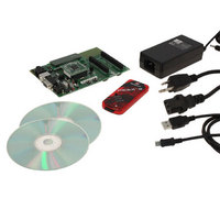
DV164136 Microchip Technology, DV164136 Datasheet - Page 8

DV164136
Manufacturer Part Number
DV164136
Description
DEVELOPMENT KIT FOR PIC18
Manufacturer
Microchip Technology
Series
PIC®r
Type
MCUr
Datasheets
1.DM183032.pdf
(38 pages)
2.DV164136.pdf
(448 pages)
3.DV164136.pdf
(6 pages)
4.DV164136.pdf
(446 pages)
5.DV164136.pdf
(4 pages)
6.DV164136.pdf
(18 pages)
Specifications of DV164136
Contents
Board, Cables, CDs, PICkit™ 3 Programmer, Power Supply
Processor To Be Evaluated
PIC18F8722, PIC18F87J11
Interface Type
RS-232, USB
Operating Supply Voltage
3.3 V, 5 V
Silicon Manufacturer
Microchip
Core Architecture
PIC
Core Sub-architecture
PIC18
Silicon Core Number
PIC18F
Silicon Family Name
PIC18F8xxx
Kit Contents
PIC18 Exp Brd PICkit 3 Cable CD PSU
Lead Free Status / RoHS Status
Lead free / RoHS Compliant
For Use With/related Products
PIC18F8722, PIC18F87J11
Lead Free Status / Rohs Status
Lead free / RoHS Compliant
Available stocks
Company
Part Number
Manufacturer
Quantity
Price
Company:
Part Number:
DV164136
Manufacturer:
MICROCHIP
Quantity:
12 000
PIC18F87J11 FAMILY
5. Module: Example 6-2: Erasing a Flash
EXAMPLE 6-2:
6. Module: Section 19.3 “SPI Mode” and
DS80495C-page 8
Note:
On page 94, an instruction to enable the write
process to memory for erasing the Flash program-
ming memory row is missing in the example. The
changed content is indicated in bold text in the
following example:
In Section 19.3 “SPI Mode” on page 223 and
Section 19.4 “I
following new note is included to describe the
procedure to disable the MSSPx module:
Required
Sequence
Disabling the MSSPx module by clearing
the SSPEN (SSPxCON1<5>) bit may not
reset the module. It is recommended to
clear the SSPxSTAT, SSPxCON1 and
SSPxCON2 registers and select the mode
prior to setting the SSPEN bit to enable
the MSSPx module.
ERASE_ROW
Program Memory Row
Section 19.4 “I
2
C™ Mode” on page 233, the
ERASING A FLASH PROGRAM MEMORY ROW
MOVLW CODE_ADDR_UPPER
MOVWF TBLPTRU
MOVLW CODE_ADDR_HIGH
MOVWF TBLPTRH
MOVLW CODE_ADDR_LOW
MOVWF TBLPTRL
BSF EECON1, WREN
BSF EECON1, FREE
BCF INTCON, GIE
MOVLW 55h
MOVWF EECON2
MOVLW 0AAh
MOVWF EECON2
BSF EECON1, WR
BSF INTCON, GIE
2
C™ Mode”
; load TBLPTR with the base
; address of the memory block
; enable write to memory
; enable Row Erase operation
; disable interrupts
; write 55h
; write 0AAh
; start erase (CPU stall)
; re-enable interrupts
7. Module: Figure 19-10: I
On page 244, the figure is replaced with the new
timing diagram provided in Figure 19-10.
Timing (Transmission, 7-Bit
Address)
2010 Microchip Technology Inc.
2
C™ Slave Mode


