C8051F064EK Silicon Laboratories Inc, C8051F064EK Datasheet - Page 327
C8051F064EK
Manufacturer Part Number
C8051F064EK
Description
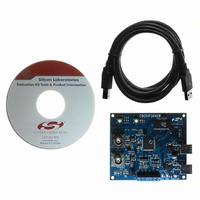
KIT EVAL FOR C8051F064
Manufacturer
Silicon Laboratories Inc
Type
MCUr
Specifications of C8051F064EK
Contents
Evaluation Board, Power Supply, USB Cables, Adapter and Documentation
Processor To Be Evaluated
C8051F06x
Interface Type
USB
Silicon Manufacturer
Silicon Labs
Core Architecture
8051
Silicon Core Number
C8051F064
Silicon Family Name
C8051F06x
Lead Free Status / RoHS Status
Contains lead / RoHS non-compliant
For Use With/related Products
C8051F064
Lead Free Status / Rohs Status
Lead free / RoHS Compliant
Other names
336-1219


Document Change List
Revision 1.1 to Revision 1.2
•
•
•
•
•
•
•
•
•
•
•
•
•
•
•
•
•
•
•
•
•
•
•
•
•
•
•
•
Added four part numbers: C8051F064, C8051F065, C8051F066, and C8051F067.
Modified all sections to describe functionality of the four new parts.
Revised and expanded Flash Chapter with clearer descriptions of Flash security features.
UART0 Chapter, Section 22.3: “FE0 in register SCON0” changed to “FE0 in register SSTA0”.
UART0 Chapter: Updated and clarified baud rate equations.
Port I/O Chapter, Section 18.2: Added a note in text body that Port 4-7 registers are all on SFR Page F.
Comparators Chapter: Updated Table 12.1 “Comparator Electrical Characteristics”.
CIP51 Chapter: Section 13.4.1: Added note regarding IDLE mode operation.
ADC2 Chapter: AD2LJST bit removed from ADC2CF register description (AD2LJST is in the ADC2CN
register).
ADC2 Chapter: Updated Table 7.1 “ADC2 Electrical Characteristics” and Figure 7.2 “Temperature Sen-
sor Transfer Function” with temperature sensor information.
ADC0/ADC1 Chapter: Tracking/Conversion timing when ADnTM = 1 is shown in Figure 5.4 and Table
5.1. References to “18” or “16” SAR clocks of tracking were removed.
DACs Chapter, Table 8.1 “DAC Electrical Characteristics”: Changed “Gain Error” to “Full-Scale Error”.
SMBus Chapter, Figure 20.9 SMB0CR: Changed “1.125” to “1.125 * 10^6”.
PCA Chapter, Figure 25.12 PCA0CPMn: Bit 0 name changed to “ECCFn” (from incorrect “EECFn”).
JTAG Chapter, Figure 26.3 FLASHCON: Bit 7 description corrected. Bit 7 is SFLE, allowing access to
the Scratchpad memory area.
CAN Chapter: Added text “The CAN controller’s clock (f
is equal to the CIP-51 MCU’s clock (SYSCLK).”
Table 4.1 “Pin Descriptions”, MONEN: Added text “Recommended configuration is to connect directly
to VDD.”
Timers Chapter: All references to “DCEN” and “DECEN” corrected to “DCENn”.
Timers Chapter, Equation 24.1: Equation was corrected to “Fsq = Ftclk / (2*(65536-RCAPn))”. This
equation is valid for a timer counting up or down.
Timers Chapter, Figure 24.14 TMRnCF: Corrected Bit 1 description. For square-wave output, CP/RLn
= 0, C/Tn = 0, TnOE = 1.
VREF Chapters: Added VREF Power Supply Current to VREF Electrical Characteristics Tables.
PCA Chapter: Added Note about writing PCA0CPLn and PCA0CPHn to sections for SW Timer Mode,
High-Speed Output Mode, Frequency Output Mode, 8-bit PWM Mode, and 16-bit PWM Mode.
Oscillators Chapter, Table 15.1 “Internal Oscillator Electrical Characteristics”: Updated typical supply
current.
Table 3.1 “Global DC Electrical Characteristics”, Updated supply current numbers with additional char-
acterization data.
ADC0/ADC1 Chapter: Table 5.2 “ADC0 and ADC1 Electrical Characteristics”, Updated supply current
numbers with additional characterization data.
ADC0/ADC1 Chapter: Table 5.3 “Voltage Reference 0 and 1 Electrical Characteristics”, Updated Out-
put Voltage numbers with characterization data.
Figure 4.3 “TQFP-100 Package Drawing”, Added “L” Dimension.
Figure 4.6 “TQFP-64 Package Drawing”, Added “L” Dimension.
Rev. 1.2
C8051F060/1/2/3/4/5/6/7
sys
, or CAN_CLK in the C_CAN User’s Guide)
327
Related parts for C8051F064EK
Image
Part Number
Description
Manufacturer
Datasheet
Request
R

Part Number:
Description:
SMD/C°/SINGLE-ENDED OUTPUT SILICON OSCILLATOR
Manufacturer:
Silicon Laboratories Inc
Part Number:
Description:
Manufacturer:
Silicon Laboratories Inc
Datasheet:
Part Number:
Description:
N/A N/A/SI4010 AES KEYFOB DEMO WITH LCD RX
Manufacturer:
Silicon Laboratories Inc
Datasheet:
Part Number:
Description:
N/A N/A/SI4010 SIMPLIFIED KEY FOB DEMO WITH LED RX
Manufacturer:
Silicon Laboratories Inc
Datasheet:
Part Number:
Description:
N/A/-40 TO 85 OC/EZLINK MODULE; F930/4432 HIGH BAND (REV E/B1)
Manufacturer:
Silicon Laboratories Inc
Part Number:
Description:
EZLink Module; F930/4432 Low Band (rev e/B1)
Manufacturer:
Silicon Laboratories Inc
Part Number:
Description:
I°/4460 10 DBM RADIO TEST CARD 434 MHZ
Manufacturer:
Silicon Laboratories Inc
Part Number:
Description:
I°/4461 14 DBM RADIO TEST CARD 868 MHZ
Manufacturer:
Silicon Laboratories Inc
Part Number:
Description:
I°/4463 20 DBM RFSWITCH RADIO TEST CARD 460 MHZ
Manufacturer:
Silicon Laboratories Inc
Part Number:
Description:
I°/4463 20 DBM RADIO TEST CARD 868 MHZ
Manufacturer:
Silicon Laboratories Inc
Part Number:
Description:
I°/4463 27 DBM RADIO TEST CARD 868 MHZ
Manufacturer:
Silicon Laboratories Inc
Part Number:
Description:
I°/4463 SKYWORKS 30 DBM RADIO TEST CARD 915 MHZ
Manufacturer:
Silicon Laboratories Inc
Part Number:
Description:
N/A N/A/-40 TO 85 OC/4463 RFMD 30 DBM RADIO TEST CARD 915 MHZ
Manufacturer:
Silicon Laboratories Inc
Part Number:
Description:
I°/4463 20 DBM RADIO TEST CARD 169 MHZ
Manufacturer:
Silicon Laboratories Inc