DEMO9S08LG32 Freescale Semiconductor, DEMO9S08LG32 Datasheet - Page 14
DEMO9S08LG32
Manufacturer Part Number
DEMO9S08LG32
Description
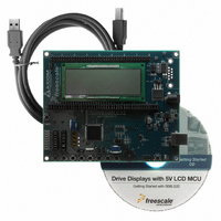
DEMO BOARD FOR LG32 FAMILY MCU
Manufacturer
Freescale Semiconductor
Type
MCUr
Datasheets
1.DEMO9S08LG32.pdf
(50 pages)
2.DEMO9S08LG32.pdf
(25 pages)
3.DEMO9S08LG32.pdf
(10 pages)
4.DEMO9S08LG32.pdf
(2 pages)
5.CWS-H08-STDED-CX.pdf
(4 pages)
Specifications of DEMO9S08LG32
Contents
Board, CD
Processor To Be Evaluated
MC9S08LG32x
Data Bus Width
8 bit
Interface Type
USB
Maximum Operating Temperature
+ 85 C
Minimum Operating Temperature
- 40 C
Silicon Manufacturer
Freescale
Core Architecture
HCS08
Core Sub-architecture
HCS08
Silicon Core Number
MC9S08
Silicon Family Name
S08LG
Rohs Compliant
Yes
For Use With/related Products
MC9S08LG32
Lead Free Status / RoHS Status
Contains lead / RoHS non-compliant


Electrical Characteristics
1
2
3
4
5
6
7
14
Num C
14
15
16
17
18
19
20
21
22
23
24
25
Typical values are measured at 25 °C. Characterized, not tested
Measured with V
Measured with V
Measured with V
All functional non-supply pins, except for PTC6 are internally clamped to V
Input must be current limited to the value specified. To determine the value of the required current-limiting resistor, calculate
resistance values for positive and negative clamp voltages, then use the larger of the two values.
Power supply must maintain regulation within operating V
conditions. If the positive injection current (V
result in external power supply going out of regulation. Ensure that external V
injection current. This will be the greatest risk when the MCU is not consuming power. For instance, if no system clock is
present, or if clock rate is very low (which would reduce overall power consumption).
D DC injection
C Input Capacitance, all non-supply pins
C RAM retention voltage
D POR rearm time
P POR rearm voltage
P Low-voltage detection threshold — high range
P Low-voltage detection threshold — low range
P Low-voltage warning threshold — high range 1
P Low-voltage warning threshold — high range 0
P Low-voltage warning threshold — low range 1
P Low-voltage warning threshold — low range 0
P Low-voltage inhibit reset/recover hysteresis
current
V
IN
< V
5, 6, 7
V
In
In
In
SS
DD
= V
= V
= V
, V
DD
SS
DD
IN
.
>
.
or V
Single pin limit
Total MCU limit, includes sum of
all stressed pins
SS
.
Characteristic
Table 8. DC Characteristics (continued)
MC9S08LG32 Series Data Sheet, Rev. 7
In
> V
DD
) is greater than I
DD
V
V
V
V
V
V
V
V
V
V
V
V
range during instantaneous and operating maximum current
DD
DD
DD
DD
DD
DD
DD
DD
DD
DD
DD
DD
falling
falling
falling
falling
falling
falling
rising
rising
rising
rising
rising
rising
5 V
3 V
DD
, the injection current may flow out of V
Symbol
V
V
V
V
V
V
V
V
t
V
SS
POR
C
LVW3
LVW2
LVW1
LVW0
LVD1
LVD0
I
RAM
POR
IC
hys
DD
In
and V
load will shunt current greater than maximum
DD
.
2.48
2.54
2.84
2.90
2.66
2.72
Min
0.9
3.9
4.0
4.5
4.6
4.2
4.3
10
—
—
—
—
2
Typ
2.56
2.62
2.92
2.98
2.74
2.80
100
1.4
4.0
4.1
4.6
4.7
4.3
4.4
60
—
—
—
—
—
Freescale Semiconductor
1
Max
2.64
2.70
3.00
3.06
2.82
2.88
2.0
4.1
4.2
4.7
4.8
4.4
4.5
25
—
—
—
2
8
DD
and could
Unit
mA
mA
mV
pF
μs
V
V
V
V
V
V
V
V
Related parts for DEMO9S08LG32
Image
Part Number
Description
Manufacturer
Datasheet
Request
R

Part Number:
Description:
Manufacturer:
Freescale Semiconductor, Inc
Datasheet:
Part Number:
Description:
Manufacturer:
Freescale Semiconductor, Inc
Datasheet:
Part Number:
Description:
Manufacturer:
Freescale Semiconductor, Inc
Datasheet:
Part Number:
Description:
Manufacturer:
Freescale Semiconductor, Inc
Datasheet:
Part Number:
Description:
Manufacturer:
Freescale Semiconductor, Inc
Datasheet:
Part Number:
Description:
Manufacturer:
Freescale Semiconductor, Inc
Datasheet:
Part Number:
Description:
Manufacturer:
Freescale Semiconductor, Inc
Datasheet:
Part Number:
Description:
Manufacturer:
Freescale Semiconductor, Inc
Datasheet:
Part Number:
Description:
Manufacturer:
Freescale Semiconductor, Inc
Datasheet:
Part Number:
Description:
Manufacturer:
Freescale Semiconductor, Inc
Datasheet:
Part Number:
Description:
Manufacturer:
Freescale Semiconductor, Inc
Datasheet:
Part Number:
Description:
Manufacturer:
Freescale Semiconductor, Inc
Datasheet:
Part Number:
Description:
Manufacturer:
Freescale Semiconductor, Inc
Datasheet:
Part Number:
Description:
Manufacturer:
Freescale Semiconductor, Inc
Datasheet:
Part Number:
Description:
Manufacturer:
Freescale Semiconductor, Inc
Datasheet: