C8051T600DK Silicon Laboratories Inc, C8051T600DK Datasheet - Page 44
C8051T600DK
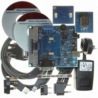
Manufacturer Part Number
C8051T600DK
Description
KIT DEV FOR C8051T60X MCU'S
Manufacturer
Silicon Laboratories Inc
Type
MCUr
Specifications of C8051T600DK
Contents
Evaluation Board, Power Supply, USB Cables, Adapter and Documentation
Processor To Be Evaluated
C8051T60x
Interface Type
USB
Lead Free Status / RoHS Status
Contains lead / RoHS non-compliant
For Use With/related Products
C8051T600, C8051T601, C8051T602, C8051T603, C8051T604, C8051T605
Lead Free Status / Rohs Status
Lead free / RoHS Compliant
Other names
336-1404


C8051T600/1/2/3/4/5/6
SFR Definition 9.1. ADC0CF: ADC0 Configuration
SFR Address = 0xBC
44
Name
Reset
7:3 AD0SC[4:0] ADC0 SAR Conversion Clock Period Bits.
Bit
Type
2
1
0
Bit
AMP0GN0 ADC Gain Control Bit.
AD0LJST
AD08BE
Name
7
1
SAR Conversion clock is derived from system clock by the following equation, where
AD0SC refers to the 5-bit value held in bits AD0SC4–0. SAR Conversion clock
requirements are given in the ADC specification table.
Note: If the Memory Power Controller is enabled (MPCE = '1'), AD0SC must be set to at least
ADC0 Left Justify Select.
0: Data in ADC0H:ADC0L registers are right-justified.
1: Data in ADC0H:ADC0L registers are left-justified.
Note: The AD0LJST bit is only valid for 10-bit mode (AD08BE = 0).
8-Bit Mode Enable.
0: ADC operates in 10-bit mode (normal).
1: ADC operates in 8-bit mode.
Note: When AD08BE is set to 1, the AD0LJST bit is ignored.
0: Gain = 0.5
1: Gain = 1
AD0SC
6
1
"00001" for proper ADC operation.
=
AD0SC[4:0]
SYSCLK
---------------------- - 1
CLK
R/W
5
1
SAR
–
Rev. 1.2
4
1
Function
3
1
AD0LJST
R/W
2
0
AD08BE
R/W
1
0
AMP0GN0
R/W
0
1
Related parts for C8051T600DK
Image
Part Number
Description
Manufacturer
Datasheet
Request
R

Part Number:
Description:
SMD/C°/SINGLE-ENDED OUTPUT SILICON OSCILLATOR
Manufacturer:
Silicon Laboratories Inc
Part Number:
Description:
Manufacturer:
Silicon Laboratories Inc
Datasheet:
Part Number:
Description:
N/A N/A/SI4010 AES KEYFOB DEMO WITH LCD RX
Manufacturer:
Silicon Laboratories Inc
Datasheet:
Part Number:
Description:
N/A N/A/SI4010 SIMPLIFIED KEY FOB DEMO WITH LED RX
Manufacturer:
Silicon Laboratories Inc
Datasheet:
Part Number:
Description:
N/A/-40 TO 85 OC/EZLINK MODULE; F930/4432 HIGH BAND (REV E/B1)
Manufacturer:
Silicon Laboratories Inc
Part Number:
Description:
EZLink Module; F930/4432 Low Band (rev e/B1)
Manufacturer:
Silicon Laboratories Inc
Part Number:
Description:
I°/4460 10 DBM RADIO TEST CARD 434 MHZ
Manufacturer:
Silicon Laboratories Inc
Part Number:
Description:
I°/4461 14 DBM RADIO TEST CARD 868 MHZ
Manufacturer:
Silicon Laboratories Inc
Part Number:
Description:
I°/4463 20 DBM RFSWITCH RADIO TEST CARD 460 MHZ
Manufacturer:
Silicon Laboratories Inc
Part Number:
Description:
I°/4463 20 DBM RADIO TEST CARD 868 MHZ
Manufacturer:
Silicon Laboratories Inc
Part Number:
Description:
I°/4463 27 DBM RADIO TEST CARD 868 MHZ
Manufacturer:
Silicon Laboratories Inc
Part Number:
Description:
I°/4463 SKYWORKS 30 DBM RADIO TEST CARD 915 MHZ
Manufacturer:
Silicon Laboratories Inc
Part Number:
Description:
N/A N/A/-40 TO 85 OC/4463 RFMD 30 DBM RADIO TEST CARD 915 MHZ
Manufacturer:
Silicon Laboratories Inc
Part Number:
Description:
I°/4463 20 DBM RADIO TEST CARD 169 MHZ
Manufacturer:
Silicon Laboratories Inc