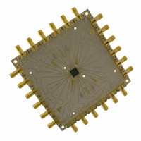
NBSG111BAEVB ON Semiconductor, NBSG111BAEVB Datasheet - Page 6
NBSG111BAEVB
Manufacturer Part Number
NBSG111BAEVB
Description
BOARD EVALUATION BBG NBSG111BA
Manufacturer
ON Semiconductor
Specifications of NBSG111BAEVB
Main Purpose
Clock/Data Driver
Utilized Ic / Part
NBSG111
Primary Attributes
W/RSECL Outputs
Technology Type
Evaluation Board
Lead Free Status / RoHS Status
Contains lead / RoHS non-compliant
For Use With/related Products
NBSG111
Other names
NBSG111BAEVB
NBSG111BAEVBOS
NBSG111BAEVBOS


Setup Test Configurations For Single−Ended Operation
Single−Ended Mode – Small Signal
Step 2:
Single−Ended Mode – Large Signal
Step 2:
Step 3:
Step 3:
Input Setup
Output Setup
Input Setup
Output Setup
NOTE:
2a: Calibrate VNA from 1.0 GHz to 12 GHz.
2b: Set input level to –35 dBm at the input of DUT.
3a: Set display to measure S21 and record data.
2a: Calibrate VNA from 1.0 GHz to 12 GHz.
2b: Set input levels to +2 dBm (500 mV) at the input of DUT.
3a: Set display to measure S21 and record data.
Figure 5. NBSG111 Board Setup – Frequency Domain (Single−Ended Mode)
PORT 1
All differential cable pairs must be matched.
Due to simplifcation of the block diagram CLK1/CLK1 and Q1 − Q8 connections are not shown.
GND
V
EE
50 W
= −1.3 V (3.3 V op)
V
CLK0
CLK0
V
V
CC
CC
EE
= 2.0 V
Vector Network Analyzer
NBSG111BAEVB
http://onsemi.com
SEL
EN
V
V
CC
CC
SEL
6
EN
Float
Float
V
V
TT
GND
GND
TT
= 0 V
= 0 V
Q0
Q0
Q9
Q9
GND
Bias T
50 W
GND
GND
50 W
50 W
PORT 2
GND
* Q0 − Q9 Outputs
50 W
Related parts for NBSG111BAEVB
Image
Part Number
Description
Manufacturer
Datasheet
Request
R

Part Number:
Description:
2.5v/3.3v Sige Differential 1 10 Clock/data Driver With Rsecl Outputs
Manufacturer:
ON Semiconductor
Datasheet:
Part Number:
Description:
ON Semiconductor [VOLTAGE REGULATOR]
Manufacturer:
ON Semiconductor
Datasheet:
Part Number:
Description:
357-036-542-201 CARDEDGE 36POS DL .156 BLK LOPRO
Manufacturer:
ON Semiconductor
Datasheet:
Part Number:
Description:
357-036-542-201 CARDEDGE 36POS DL .156 BLK LOPRO
Manufacturer:
ON Semiconductor
Datasheet:
Part Number:
Description:
357-036-542-201 CARDEDGE 36POS DL .156 BLK LOPRO
Manufacturer:
ON Semiconductor
Datasheet:
Part Number:
Description:
357-036-542-201 CARDEDGE 36POS DL .156 BLK LOPRO
Manufacturer:
ON Semiconductor
Datasheet:
Part Number:
Description:
357-036-542-201 CARDEDGE 36POS DL .156 BLK LOPRO
Manufacturer:
ON Semiconductor
Datasheet:
Part Number:
Description:
357-036-542-201 CARDEDGE 36POS DL .156 BLK LOPRO
Manufacturer:
ON Semiconductor
Datasheet:
Part Number:
Description:
357-036-542-201 CARDEDGE 36POS DL .156 BLK LOPRO
Manufacturer:
ON Semiconductor
Datasheet:
Part Number:
Description:
357-036-542-201 CARDEDGE 36POS DL .156 BLK LOPRO
Manufacturer:
ON Semiconductor
Datasheet:
Part Number:
Description:
357-036-542-201 CARDEDGE 36POS DL .156 BLK LOPRO
Manufacturer:
ON Semiconductor
Datasheet:
Part Number:
Description:
357-036-542-201 CARDEDGE 36POS DL .156 BLK LOPRO
Manufacturer:
ON Semiconductor
Datasheet:
Part Number:
Description:
Manufacturer:
ON Semiconductor
Datasheet:
Part Number:
Description:
Manufacturer:
ON Semiconductor
Datasheet: