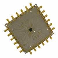
NBSG111BAEVB ON Semiconductor, NBSG111BAEVB Datasheet - Page 9

NBSG111BAEVB
Manufacturer Part Number
NBSG111BAEVB
Description
BOARD EVALUATION BBG NBSG111BA
Manufacturer
ON Semiconductor
Specifications of NBSG111BAEVB
Main Purpose
Clock/Data Driver
Utilized Ic / Part
NBSG111
Primary Attributes
W/RSECL Outputs
Technology Type
Evaluation Board
Lead Free Status / RoHS Status
Contains lead / RoHS non-compliant
For Use With/related Products
NBSG111
Other names
NBSG111BAEVB
NBSG111BAEVBOS
NBSG111BAEVBOS
(Total Pk−Pk system jitter including signal generator is 28 ps. Device Pk−Pk jitter is typically 14 ps.)
550
450
350
250
150
Figure 10. NBSG111: Eye Diagram at 6 Gbps with PRBS 2^31−1
Figure 9. Output Voltage Amplitude (V
1
Input Frequency (f
EXAMPLE MEASUREMENTS IN TIME DOMAIN
RMS JITTER (ps)
Q AMP (mV)
2
INPUT FREQUENCY (GHz)
NBSG111BAEVB
http://onsemi.com
in
) at Ambient Temperature (Typical)
3
2.5 V
3.3 V
9
4
OUTPP
) / RMS Jitter vs.
5
6
10.0
9.0
8.0
7.0
6.0
5.0
4.0
3.0
2.0
1.0
0.0


