ATAVRAUTO102 Atmel, ATAVRAUTO102 Datasheet - Page 9
ATAVRAUTO102
Manufacturer Part Number
ATAVRAUTO102
Description
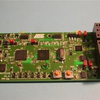
DEBUGGER KIT
Manufacturer
Atmel
Series
AVR®r
Type
Evaluation kitr
Datasheet
1.ATAVRAUTO102.pdf
(18 pages)
Specifications of ATAVRAUTO102
Contents
2 Boards, cable and software
Processor To Be Evaluated
AT90CAN128 and AT90USB1287
Interface Type
USB
For Use With/related Products
AT90CAN128
Lead Free Status / RoHS Status
Lead free / RoHS Compliant
Other names
Q3524911


3.2.2
3.2.3
ATAVRAUTO102 User Guide
Programming with
AVR ISP via SPI
Programming with
AVR JTAGICE mkII
Both the Flash and EEPROM memory arrays can be programmed using the serial SPI
bus while RESET is pulled to GND. The serial interface consists of pins SCK, MOSI
(input) and MISO (output). After RESET is set low, the Programming Enable instruction
needs to be executed first before program/erase operations can be executed. Note that
throughout the description about Serial downloading, MOSI and MISO are used to
describe the serial data in and serial data out respectively. For AT90CAN128 these pins
are mapped to PDI (PE0) and PDO (PE1).
To program the device using AVR ISP programmer, connect the AVR ISP to the adaptor
(ATAVRAUTO900) and connect the adaptor to the connector of the ATAVRAUTO102.
Programming the ATAVRAUTO102 using ATAVRAUTO 900
The AT90CAN128 can be programmed using specific JTAG link: 3-wire debug-wire
interface. To use the AVR JTAGICE mkII with an ATAVRAUTO100 an optional adaptor
should be used. Then the JTAG probe can be connected to the ATAVRAUTO100 as
shown in the following figure.
JTAGICE mkII probe connection through JTAG interface.
7720A–AVR–06/07
3-7
Related parts for ATAVRAUTO102
Image
Part Number
Description
Manufacturer
Datasheet
Request
R


Part Number:
Description:
DEV KIT FOR AVR/AVR32
Manufacturer:
Atmel
Datasheet:

Part Number:
Description:
INTERVAL AND WIPE/WASH WIPER CONTROL IC WITH DELAY
Manufacturer:
ATMEL Corporation
Datasheet:
Part Number:
Description:
Low-Voltage Voice-Switched IC for Hands-Free Operation
Manufacturer:
ATMEL Corporation
Datasheet:
Part Number:
Description:
MONOLITHIC INTEGRATED FEATUREPHONE CIRCUIT
Manufacturer:
ATMEL Corporation
Datasheet:
Part Number:
Description:
AM-FM Receiver IC U4255BM-M
Manufacturer:
ATMEL Corporation
Datasheet:
Part Number:
Description:
Monolithic Integrated Feature Phone Circuit
Manufacturer:
ATMEL Corporation
Datasheet:
Part Number:
Description:
Multistandard Video-IF and Quasi Parallel Sound Processing
Manufacturer:
ATMEL Corporation
Datasheet:
Part Number:
Description:
High-performance EE PLD
Manufacturer:
ATMEL Corporation
Datasheet:
Part Number:
Description:
8-bit Flash Microcontroller
Manufacturer:
ATMEL Corporation
Datasheet:
Part Number:
Description:
2-Wire Serial EEPROM
Manufacturer:
ATMEL Corporation
Datasheet: