AD9777-EB Analog Devices Inc, AD9777-EB Datasheet - Page 23
AD9777-EB
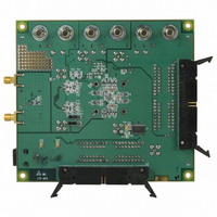
Manufacturer Part Number
AD9777-EB
Description
BOARD EVAL FOR AD9777
Manufacturer
Analog Devices Inc
Series
TxDAC+®r
Datasheet
1.AD9777BSVZ.pdf
(60 pages)
Specifications of AD9777-EB
Rohs Status
RoHS non-compliant
Number Of Dac's
2
Number Of Bits
16
Outputs And Type
2, Differential
Sampling Rate (per Second)
160M
Data Interface
Parallel
Settling Time
11ns
Dac Type
Current
Voltage Supply Source
Analog and Digital
Operating Temperature
-40°C ~ 85°C
Utilized Ic / Part
AD9777


INSTRUCTION BYTE
The instruction byte contains the information shown below.
N1
0
0
1
1
R/W
Bit 7 of the instruction byte determines whether a read or a
write data transfer occurs after the instruction byte write. Logic
1 indicates read operation. Logic 0 indicates a write operation.
N1, N0
Bit 6 and Bit 5 of the instruction byte determine the number of
bytes to be transferred during the data transfer cycle. The bit
decodes are shown in the following table.
MSB
I7
R/W
A4, A3, A2, A1, A0
Bit 4, Bit 3, Bit 2, Bit 1, and Bit 0 of the instruction byte
determine which register is accessed during the data transfer
portion of the communications cycle. For multibyte transfers,
this address is the starting byte address. The remaining register
addresses are generated by the AD9777.
SERIAL INTERFACE PORT PIN DESCRIPTIONS
SPI_CLK (Pin 55)—Serial Clock
The serial clock pin is used to synchronize data to and from the
AD9777 and to run the internal state machines. SPI_CLK
maximum frequency is 15 MHz. All data input to the AD9777
is registered on the rising edge of SPI_CLK. All data is driven
out of the AD9777 on the falling edge of SCLK.
I6
N1
N0
0
1
0
1
I5
N0
Description
Transfer 1 Byte
Transfer 2 Bytes
Transfer 3 Bytes
Transfer 4 Bytes
I4
A4
I3
A3
I2
A2
I1
A1
LSB
I0
A0
Rev. C | Page 23 of 60
SPI_CSB (Pin 56)—Chip Select
Active low input starts and gates a communication cycle. It
allows more than one device to be used on the same serial
communications lines. The SPI_SDO and SPI_SDIO pins go to
a high impedance state when this input is high. Chip select
should stay low during the entire communication cycle.
SPI_SDIO (Pin 54)—Serial Data I/O
Data is always written into the AD9777 on this pin. However,
this pin can be used as a bidirectional data line. Bit 7 of Register
Address 00h controls the configuration of this pin. The default
is Logic 0, which configures the SPI_SDIO pin as
unidirectional.
SPI_SDO (Pin 53)—Serial Data Out
Data is read from this pin for protocols that use separate lines
for transmitting and receiving data. In the case where the
AD9777 operates in a single bidirectional I/O mode, this pin
does not output data and is set to a high impedance state.
MSB/LSB TRANSFERS
The AD9777 serial port can support both most significant bit
(MSB) first or least significant bit (LSB) first data formats. This
functionality is controlled by the LSB first bit in Register 0. The
default is MSB first.
When this bit is set active high, the AD9777 serial port is in LSB
first format. In LSB first mode, the instruction byte and data
bytes must be written from LSB to MSB. In LSB first mode, the
serial port internal byte address generator increments for each
byte of the multibyte communication cycle.
When this bit is set default low, the AD9777 serial port is in
MSB first format. In MSB first mode, the instruction byte and
data bytes must be written from MSB to LSB. In MSB first
mode, the serial port internal byte address generator decre-
ments for each byte of the multibyte communication cycle.
When incrementing from 1Fh, the address generator changes to
00h. When decrementing from 00h, the address generator
changes to 1Fh.
AD9777
Related parts for AD9777-EB
Image
Part Number
Description
Manufacturer
Datasheet
Request
R

Part Number:
Description:
16Bit 400 MSPS Dual TxDAC+ D/A Converter
Manufacturer:
Analog Devices Inc
Datasheet:

Part Number:
Description:
±1.7g Dual-Axis IMEMS Accelerometer Evaluation Board
Manufacturer:
Analog Devices Inc
Datasheet:
Part Number:
Description:
Inertial Sensor Evaluation System
Manufacturer:
Analog Devices Inc
Datasheet:
Part Number:
Description:
Manufacturer:
Analog Devices Inc
Datasheet:
Part Number:
Description:
Manufacturer:
Analog Devices Inc
Datasheet:
Part Number:
Description:
Manufacturer:
Analog Devices Inc
Datasheet:
Part Number:
Description:
Manufacturer:
Analog Devices Inc
Datasheet:
Part Number:
Description:
Manufacturer:
Analog Devices Inc
Datasheet:
Part Number:
Description:
Manufacturer:
Analog Devices Inc
Datasheet:
Part Number:
Description:
Manufacturer:
Analog Devices Inc
Datasheet:
Part Number:
Description:
Manufacturer:
Analog Devices Inc
Datasheet:
Part Number:
Description:
Manufacturer:
Analog Devices Inc
Datasheet:
Part Number:
Description:
Manufacturer:
Analog Devices Inc
Datasheet: