AD9777-EB Analog Devices Inc, AD9777-EB Datasheet - Page 29
AD9777-EB
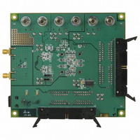
Manufacturer Part Number
AD9777-EB
Description
BOARD EVAL FOR AD9777
Manufacturer
Analog Devices Inc
Series
TxDAC+®r
Datasheet
1.AD9777BSVZ.pdf
(60 pages)
Specifications of AD9777-EB
Rohs Status
RoHS non-compliant
Number Of Dac's
2
Number Of Bits
16
Outputs And Type
2, Differential
Sampling Rate (per Second)
160M
Data Interface
Parallel
Settling Time
11ns
Dac Type
Current
Voltage Supply Source
Analog and Digital
Operating Temperature
-40°C ~ 85°C
Utilized Ic / Part
AD9777


POWER DISSIPATION
The AD9777 has three voltage supplies: DVDD, AVDD, and
CLKVDD. Figure 49, Figure 50, and Figure 51 show the current
required from each of these supplies when each is set to the
3.3 V nominal specified for the AD9777. Power dissipation (P
can easily be extracted by multiplying the given curves by 3.3.
As Figure 49 shows, I
rate, the interpolation rate, and the activation of the internal
digital modulator. I
modulation rate by itself. In Figure 50, I
type of sensitivity to data, interpolation rate, and the modulator
function but to a much lesser degree (<10%). In Figure 51,
I
small percentage of the overall AD9777 supply current
requirement.
CLKVDD
76.0
75.5
75.0
74.5
74.0
73.5
73.0
72.5
72.0
400
350
300
250
200
150
100
50
0
varies over a wide range yet is responsible for only a
0
0
Figure 49. I
Figure 50. I
8×, (MOD. ON)
8×, (MOD. ON)
DVDD
AVDD
8×
8×
50
50
DVDD
vs. f
vs. f
DVDD
, however, is relatively insensitive to the
DATA
DATA
4×
is very dependent on the input data
4×
vs. Interpolation Rate, PLL Disabled
vs. Interpolation Rate, PLL Disabled
f
f
DATA
DATA
4×, (MOD. ON)
100
100
(MHz)
(MHz)
4×, (MOD. ON)
AVDD
2×, (MOD. ON)
150
150
2×, (MOD. ON)
shows the same
1×
1×
2×
2×
200
200
Rev. C | Page 29 of 60
D
)
SLEEP/POWER-DOWN MODES
(Control Register 00h, Bit 3 and Bit 4)
The AD9777 provides two methods for programmable
reduction in power savings. The sleep mode, when activated,
turns off the DAC output currents but the rest of the chip
remains functioning. When coming out of sleep mode, the
AD9777 immediately returns to full operation. Power-down
mode, on the other hand, turns off all analog and digital
circuitry in the AD9777 except for the SPI port. When
returning from power-down mode, enough clock cycles must
be allowed to flush the digital filters of random data acquired
during the power-down cycle. Note that optimal performance
with the PLL enabled is achieved with the UCO in the PLL
control loop running at 450 MHz to 550 MHz.
TWO PORT DATA INPUT MODE
The digital data input ports can be configured as two
independent ports or as a single (one-port mode) port. In the
two-port mode, data at the two input ports is latched into the
AD9777 on every rising edge of the data rate clock (DATACLK).
In addition, in the two-port mode, the AD9777 can be
programmed to generate an externally available DATACLK for
the purpose of data synchronization. This data rate clock can be
programmed to be available at either Pin 8 (DATACLK/
PLL_LOCK) or Pin 53 (SPI_SDO). Because Pin 8 can also
function as a PLL lock indicator when the PLL is enabled, there
are several options for configuring Pin 8 and Pin 53. The
following information describes these options.
PLL Off (Register 4, Bit 7 = 0)
Register 3, Bit 7 = 0; DATACLK out of Pin 8.
Register 3, Bit 7 = 1; DATACLK out of Pin 53.
PLL On (Register 4, Bit 7 = 1)
Register 3, Bit 7 = 0, Register 1, Bit 0 = 0; PLL lock indicator out
of Pin 8.
35
30
25
20
15
10
5
0
Figure 51. I
0
CLKVDD
50
8×
vs. f
DATA
4×
f
vs. Interpolation Rate, PLL Disabled
DATA
100
(MHz)
150
2×
1×
AD9777
200
Related parts for AD9777-EB
Image
Part Number
Description
Manufacturer
Datasheet
Request
R

Part Number:
Description:
16Bit 400 MSPS Dual TxDAC+ D/A Converter
Manufacturer:
Analog Devices Inc
Datasheet:

Part Number:
Description:
±1.7g Dual-Axis IMEMS Accelerometer Evaluation Board
Manufacturer:
Analog Devices Inc
Datasheet:
Part Number:
Description:
Inertial Sensor Evaluation System
Manufacturer:
Analog Devices Inc
Datasheet:
Part Number:
Description:
Manufacturer:
Analog Devices Inc
Datasheet:
Part Number:
Description:
Manufacturer:
Analog Devices Inc
Datasheet:
Part Number:
Description:
Manufacturer:
Analog Devices Inc
Datasheet:
Part Number:
Description:
Manufacturer:
Analog Devices Inc
Datasheet:
Part Number:
Description:
Manufacturer:
Analog Devices Inc
Datasheet:
Part Number:
Description:
Manufacturer:
Analog Devices Inc
Datasheet:
Part Number:
Description:
Manufacturer:
Analog Devices Inc
Datasheet:
Part Number:
Description:
Manufacturer:
Analog Devices Inc
Datasheet:
Part Number:
Description:
Manufacturer:
Analog Devices Inc
Datasheet:
Part Number:
Description:
Manufacturer:
Analog Devices Inc
Datasheet: