AD9777-EB Analog Devices Inc, AD9777-EB Datasheet - Page 25
AD9777-EB
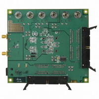
Manufacturer Part Number
AD9777-EB
Description
BOARD EVAL FOR AD9777
Manufacturer
Analog Devices Inc
Series
TxDAC+®r
Datasheet
1.AD9777BSVZ.pdf
(60 pages)
Specifications of AD9777-EB
Rohs Status
RoHS non-compliant
Number Of Dac's
2
Number Of Bits
16
Outputs And Type
2, Differential
Sampling Rate (per Second)
160M
Data Interface
Parallel
Settling Time
11ns
Dac Type
Current
Voltage Supply Source
Analog and Digital
Operating Temperature
-40°C ~ 85°C
Utilized Ic / Part
AD9777


NOTES ON SERIAL PORT OPERATION
The AD9777 serial port configuration bits reside in Bit 6 and
Bit 7 of Register Address 00h. It is important to note that the
configuration changes immediately upon writing to the last bit
of the register. For multibyte transfers, writing to this register
may occur during the middle of the communication cycle. Care
must be taken to compensate for this new configuration for the
remaining bytes of the current communication cycle.
The same considerations apply to setting the reset bit in
Register Address 00h. All other registers are set to their default
values, but the software reset does not affect the bits in Register
Address 00h.
It is recommended to use only single byte transfers when
changing serial port configurations or initiating a software
reset.
A write to Bit 1, Bit 2, and Bit 3 of Address 00h with the same
logic levels as for Bit 7, Bit 6, and Bit 5 (bit pattern: XY1001YX
binary) allows the user to reprogram a lost serial port configu-
ration and to reset the registers to their default values. A second
write to Address 00h with reset bit low and serial port configu-
ration as specified above (XY) reprograms the OSC IN
multiplier setting. A changed f
maximum of 200 f
DAC OPERATION
The dual 16-bit DAC output of the AD9777, along with the
reference circuitry, gain, and offset registers, is shown in Figure
37 and Figure 38. Note that an external reference can be used by
simply overdriving the internal reference with the external
reference. Referring to the transfer functions in Equation 1, a
reference current is set by the internal 1.2 V reference, the
external R
The fine gain DAC subtracts a small amount from this and the
result is input to IDAC and QDAC, where it is scaled by an
amount equal to 1024/24. Figure 39 and Figure 40 show the
scaling effect of the coarse and fine adjust DACs. IDAC and
QDAC are PMOS current source arrays, segmented in a 5-4-7
configuration. The five MSB control an array of 31 current
sources. The next four bits consist of 15 current sources whose
values are all equal to 1/16 of an MSB current source. The 7
LSBs are binary weighted fractions of the middle bits’ current
sources. All current sources are switched to either I
depending on the input code.
The fine adjustment of the gain of each channel allows for im-
proved balance of QAM modulated signals, resulting in improved
modulation accuracy and image rejection. In the Interfacing with
the AD8345 Quadrature Modulator section, the performance
data shows to what degree image rejection can be improved when
the AD9777 is used with an AD8345 quadrature modulator from
Analog Devices, Inc.
SET
resistor, and the values in the coarse gain register.
MCLK
cycles (equals wake-up time).
SYSCLK
frequency is stable after a
OUTA
or I
OUTB
Rev. C | Page 25 of 60
,
The offset control defines a small current that can be added to
I
of which I
mable via Register 08h, Bit 7 (IDAC) and Register 0Ch, Bit 7
(QDAC). Figure 42 shows the scale of the offset current that can
be added to one of the complementary outputs on the IDAC
and QDAC. Offset control can be used for suppression of LO
leakage resulting from modulation of dc signal components. If
the AD9777 is dc-coupled to an external modulator, this feature
can be used to cancel the output offset on the AD9777 as well as
the input offset on the modulator. Figure 42 shows a typical
example of the effect that the offset control has on LO
suppression.
REGISTERS
OUTA
REFIO
Figure 37. DAC Outputs, Reference Current Scaling, and Gain/Offset Adjust
CONTROL
1.2VREF
GAIN
0.1µF
25
20
15
10
or I
5
0
0
OUTB
OUT
RSET1
Figure 38. Internal Reference Equivalent Circuit
FSADJ1
(not both) on the IDAC and QDAC. The selection
this offset current is directed toward is program-
Figure 39. Coarse Gain Effect on I
GAIN
GAIN
FINE
DAC
FINE
DAC
(ASSUMING RSET1, RSET2 = 1.9k Ω )
5
COARSE GAIN REGISTER CODE
84µA
0.7V
RSET2
COARSE
2R MODE
GAIN
FSADJ2
DAC
AVDD
7kΩ
10
COARSE
REGISTERS
GAIN
DAC
CONTROL
1R MODE
REFIO
GAIN
REGISTERS
REGISTERS
CONTROL
IDAC
QDAC
CONTROL
15
OFFSET
FULLSCALE
OFFSET
OFFSET
OFFSET
DAC
DAC
AD9777
20
I
I
I
I
OUTA1
OUTB1
OUTA2
OUTB2
Related parts for AD9777-EB
Image
Part Number
Description
Manufacturer
Datasheet
Request
R

Part Number:
Description:
16Bit 400 MSPS Dual TxDAC+ D/A Converter
Manufacturer:
Analog Devices Inc
Datasheet:

Part Number:
Description:
±1.7g Dual-Axis IMEMS Accelerometer Evaluation Board
Manufacturer:
Analog Devices Inc
Datasheet:
Part Number:
Description:
Inertial Sensor Evaluation System
Manufacturer:
Analog Devices Inc
Datasheet:
Part Number:
Description:
Manufacturer:
Analog Devices Inc
Datasheet:
Part Number:
Description:
Manufacturer:
Analog Devices Inc
Datasheet:
Part Number:
Description:
Manufacturer:
Analog Devices Inc
Datasheet:
Part Number:
Description:
Manufacturer:
Analog Devices Inc
Datasheet:
Part Number:
Description:
Manufacturer:
Analog Devices Inc
Datasheet:
Part Number:
Description:
Manufacturer:
Analog Devices Inc
Datasheet:
Part Number:
Description:
Manufacturer:
Analog Devices Inc
Datasheet:
Part Number:
Description:
Manufacturer:
Analog Devices Inc
Datasheet:
Part Number:
Description:
Manufacturer:
Analog Devices Inc
Datasheet:
Part Number:
Description:
Manufacturer:
Analog Devices Inc
Datasheet: