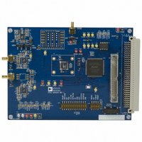
EVAL-AD7655CB Analog Devices Inc, EVAL-AD7655CB Datasheet - Page 17

EVAL-AD7655CB
Manufacturer Part Number
EVAL-AD7655CB
Description
BOARD EVAL FOR AD7655
Manufacturer
Analog Devices Inc
Series
PulSAR®r
Specifications of EVAL-AD7655CB
Number Of Adc's
1
Number Of Bits
16
Sampling Rate (per Second)
1M
Data Interface
Serial, Parallel
Inputs Per Adc
4 Single Ended
Input Range
0 ~ 2 V
Power (typ) @ Conditions
120mW @ 1MSPS
Voltage Supply Source
Analog and Digital
Operating Temperature
-40°C ~ 85°C
Utilized Ic / Part
AD7655
Lead Free Status / RoHS Status
Contains lead / RoHS non-compliant
Table 8. Recommended Driver Amplifiers
Amplifier
ADA4841
AD829
AD8021
AD8022
AD8605/AD8606/
AD8608/AD8615/
AD8616/ AD8618
AD8610/AD8620
VOLTAGE REFERENCE INPUT
The AD7655 requires an external 2.5 V reference. The reference
input should be applied to REF, REFA, and REFB. The voltage
reference input REF of the AD7655 has a dynamic input
impedance; it should therefore be driven by a low impedance
source with an efficient decoupling. This decoupling depends
on the choice of the voltage reference but usually consists of a
1 μF ceramic capacitor and a low ESR tantalum capacitor
connected to the REFA, REFB, and REFGND inputs with
minimum parasitic inductance. A value of 47 μF is appropriate
for the tantalum capacitor when using one of the recommended
reference voltages:
•
•
For applications using multiple AD7655s with one voltage
reference source, it is recommended that the reference source
drives each ADC in a star configuration with individual
decoupling placed as close as possible to the REF/REFGND
inputs. Also, it is recommended that a buffer, such as the
AD8031/AD8032, be used in this configuration.
Care should be taken with the reference temperature coefficient
of the voltage reference, which directly affects the full-scale
accuracy if this parameter is applicable. For instance, a
15 ppm/°C tempco of the reference changes the full-scale
accuracy by 1 LSB/°C.
POWER SUPPLY
The AD7655 uses three sets of power supply pins: an analog
5 V supply AVDD, a digital 5 V core supply DVDD, and a
digital input/output interface supply OVDD. The OVDD
supply allows direct interface with any logic working between
2.7 V and DVDD + 0.3 V. To reduce the number of supplies
needed, the digital core (DVDD) can be supplied through a
simple RC filter from the analog supply, as shown in Figure 17.
The AD7655 is independent of power supply sequencing, once
The low noise, low temperature drift AD780, ADR421,
and ADR431 voltage references
The low cost AD1582 voltage reference
Typical Application
Very low noise, low distortion, low power,
low frequency
Very low noise, low frequency
Very low noise, high frequency
Very low noise, high frequency, dual
5 V single supply, low power,
low frequency, single/dual/quad
Low bias current, low frequency,
single/dual
Rev. B | Page 17 of 28
OVDD does not exceed DVDD by more than 0.3 V, and thus is
free from supply voltage induced latch-up. Additionally, it is
very insensitive to power supply variations over a wide
frequency range, as shown in Figure 19.
POWER DISSIPATION
In impulse mode, the AD7655 automatically reduces its power
consumption at the end of each conversion phase. During the
acquisition phase, the operating currents are very low, which
allows significant power savings when the conversion rate is
reduced, as shown in Figure 20. This feature makes the AD7655
ideal for very low power battery applications.
Note that the digital interface remains active even during the
acquisition phase. To reduce the operating digital supply
currents even further, the digital inputs need to be driven close
to the power rails (that is, DVDD and DGND), and OVDD
should not exceed DVDD by more than 0.3 V.
1000
100
0.1
70
65
60
55
50
45
40
10
1
1
1
Figure 20. Power Dissipation vs. Sample Rate
Figure 19. PSRR vs. Frequency
10
SAMPLING RATE (kSPS)
10
FREQUENCY (kHz)
NORMAL
IMPULSE
100
100
1000
AD7655
10000
1000


