EVAL-AD7655CB Analog Devices Inc, EVAL-AD7655CB Datasheet - Page 7
EVAL-AD7655CB
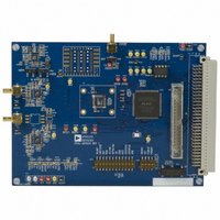
Manufacturer Part Number
EVAL-AD7655CB
Description
BOARD EVAL FOR AD7655
Manufacturer
Analog Devices Inc
Series
PulSAR®r
Specifications of EVAL-AD7655CB
Number Of Adc's
1
Number Of Bits
16
Sampling Rate (per Second)
1M
Data Interface
Serial, Parallel
Inputs Per Adc
4 Single Ended
Input Range
0 ~ 2 V
Power (typ) @ Conditions
120mW @ 1MSPS
Voltage Supply Source
Analog and Digital
Operating Temperature
-40°C ~ 85°C
Utilized Ic / Part
AD7655
Lead Free Status / RoHS Status
Contains lead / RoHS non-compliant


ABSOLUTE MAXIMUM RATINGS
Table 5.
Parameter
Analog Input
INAx
Ground Voltage Differences
Supply Voltages
Digital Inputs
Internal Power Dissipation
Internal Power Dissipation
Junction Temperature
Storage Temperature Range
Lead Temperature Range
1
2
3
ESD CAUTION
ESD (electrostatic discharge) sensitive device. Electrostatic charges as high as 4000 V readily accumulate
on the human body and test equipment and can discharge without detection. Although this product
features proprietary ESD protection circuitry, permanent damage may occur on devices subjected to
high energy electrostatic discharges. Therefore, proper ESD precautions are recommended to avoid
performance degradation or loss of functionality.
See the Analog Inputs section.
Specification is for device in free air: 48-lead LQFP, θ
θ
Specification is for device in free air: 48-lead LFCSP, θ
JC
AGND, DGND, OGND
AVDD, DVDD, OVDD
AVDD to DVDD, AVDD to OVDD
DVDD to OVDD
(Soldering 10 sec)
= 30°C/W.
1
, INBx
1
, REFx, INxN, REFGND
2
3
Values
±0.3 V
–0.3 V to +7 V
−0.3 V to +7 V
AVDD + 0.3 V to
AGND − 0.3 V
±7 V
−0.3 V to DVDD + 0.3 V
700 mW
2.5 W
150°C
−65°C to +150°C
300°C
JA
JA
= 91°C/W,
= 26°C/W.
Rev. B | Page 7 of 28
Stresses above those listed under Absolute Maximum Ratings
may cause permanent damage to the device. This is a stress
rating only; functional operation of the device at these or any
other conditions above those indicated in the operational
section of this specification is not implied. Exposure to absolute
maximum rating conditions for extended periods may affect
device reliability.
t
DELAY
*IN SERIAL INTERFACE MODES, THE SYNC, SCLK, AND
SDOUT TIMINGS ARE DEFINED WITH A MAXIMUM LOAD
C
0.8V
TO OUTPUT
L
OF 10pF; OTHERWISE, THE LOAD IS 60pF MAXIMUM.
Figure 2. Load Circuit for Digital Interface Timing
Figure 3. Voltage Reference Levels for Timing
PIN
60pF*
C
2V
0.8V
L
1.6mA
500μA
I
I
OL
OH
2V
t
DELAY
1.4V
2V
0.8V
AD7655
Related parts for EVAL-AD7655CB
Image
Part Number
Description
Manufacturer
Datasheet
Request
R

Part Number:
Description:
ENERCHIP CC EVAL KIT
Manufacturer:
Cymbet Corporation
Datasheet:

Part Number:
Description:
BOARD EVAL FOR AD976
Manufacturer:
Analog Devices Inc
Datasheet:

Part Number:
Description:
BOARD EVAL FOR ADXL345
Manufacturer:
Analog Devices Inc
Datasheet:

Part Number:
Description:
ENERCHIP CC SEH EVAL KIT
Manufacturer:
Cymbet Corporation
Datasheet:

Part Number:
Description:
ENERCHIP EP ENERGY HARVEST EVAL
Manufacturer:
Cymbet Corporation
Datasheet:

Part Number:
Description:
EVAL BOARD FOR TW6864-LB2-GR
Manufacturer:
Intersil
Datasheet:
Part Number:
Description:
EVAL BOARD FOR TW8816-LB3-GR
Manufacturer:
Intersil
Datasheet:
Part Number:
Description:
EVAL BOARD FOR TW8817-TA3-GRS
Manufacturer:
Intersil
Datasheet:

Part Number:
Description:
EVALUATION MODULE FOR ADUM4160
Manufacturer:
Analog Devices Inc
Datasheet:

Part Number:
Description:
BOARD EVALUATION ADCMP581BCP
Manufacturer:
Analog Devices Inc
Datasheet:
Part Number:
Description:
BOARD EVALUATION ADM1041
Manufacturer:
Analog Devices Inc
Datasheet:

Part Number:
Description:
EVAL BOARD FOR STM32F107VCT
Manufacturer:
STMicroelectronics
Datasheet:
Part Number:
Description:
BOARD EVAL FOR AD1954
Manufacturer:
Analog Devices Inc
Datasheet:
Part Number:
Description:
BOARD EVAL FOR AD1955
Manufacturer:
Analog Devices Inc
Datasheet:

Part Number:
Description:
BOARD EVAL FOR AD9831
Manufacturer:
Analog Devices Inc
Datasheet: