EVAL-AD7655CB Analog Devices Inc, EVAL-AD7655CB Datasheet - Page 9
EVAL-AD7655CB
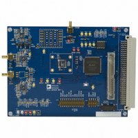
Manufacturer Part Number
EVAL-AD7655CB
Description
BOARD EVAL FOR AD7655
Manufacturer
Analog Devices Inc
Series
PulSAR®r
Specifications of EVAL-AD7655CB
Number Of Adc's
1
Number Of Bits
16
Sampling Rate (per Second)
1M
Data Interface
Serial, Parallel
Inputs Per Adc
4 Single Ended
Input Range
0 ~ 2 V
Power (typ) @ Conditions
120mW @ 1MSPS
Voltage Supply Source
Analog and Digital
Operating Temperature
-40°C ~ 85°C
Utilized Ic / Part
AD7655
Lead Free Status / RoHS Status
Contains lead / RoHS non-compliant


Pin No.
15
16
17
18
19, 36
21
22
23
24
25 to 28
29
30
31
32
33
34
Mnemonic
D[6]
or INVSCLK
D[7]
or RDC/SDIN
OGND
OVDD
DVDD
D[8]
or SDOUT
D[9]
or SCLK
D[10]
or SYNC
D[11]
or RDERROR
D[12:15]
BUSY
EOC
RD
CS
RESET
PD
Type
DI/O
DI/O
P
P
P
DO
DI/O
DO
DO
DO
DO
DO
DI
DI
DI
DI
1
Description
When SER/PAR is LOW, this output is used as Bit 6 of the parallel port data output bus.
When SER/PAR is HIGH, this input, part of the serial port, is used to invert the SCLK signal. It is active in
both master and slave modes.
When SER/PAR is LOW, this output is used as Bit 7 of the Parallel Port Data Output Bus.
When SER/PAR is HIGH, this input, part of the serial port, is used as either an external data input or a
read mode selection input, depending on the state of EXT/INT.
When EXT/INT is HIGH, RDC/SDIN can be used as a data input to daisy-chain the conversion results
from two or more ADCs onto a single SDOUT line. The digital data level on SDIN is output on SDOUT
with a delay of 32 SCLK periods after the initiation of the read sequence.
When EXT/INT is LOW, RDC/SDIN is used to select the read mode. When RDC/SDIN is HIGH, the
previous data is output on SDOUT during conversion. When RDC/SDIN is LOW, the data can be output
on SDOUT only when the conversion is complete.
Input/Output Interface Digital Power Ground.
Input/Output Interface Digital Power. Nominally at the same supply as the supply of the host interface
(5 V or 3 V).
Digital Power. Nominally at 5 V.
When SER/PAR is LOW, this output is used as Bit 8 of the Parallel Port Data Output Bus.
When SER/PAR is HIGH, this output, part of the serial port, is used as a serial data output synchronized
to SCLK. Conversion results are stored in a 32-bit on-chip register. The AD7655 provides the two
conversion results, MSB first, from its internal shift register. The order of channel outputs is controlled
by A/B. In serial mode, when EXT/INT is LOW, SDOUT is valid on both edges of SCLK.
In serial mode, when EXT/INT is HIGH:
When SER/PAR is LOW, this output is used as Bit 9 of the Parallel Port Data Output Bus.
When SER/PAR is HIGH, this pin, part of the serial port, is used as a serial data clock input or output,
depends upon the logic state of the EXT/INT pin. The active edge where the data SDOUT is updated
depends on the logic state of the INVSCLK pin.
When SER/PAR is LOW, this output is used as Bit 10 of the Parallel Port Data Output Bus.
When SER/PAR is HIGH, this output, part of the serial port, is used as a digital output frame
synchronization for use with the internal data clock (EXT/INT = Logic LOW).
When a read sequence is initiated and INVSYNC is LOW, SYNC is driven HIGH and frames SDOUT. After
the first channel is output, SYNC is pulsed LOW. When a read sequence is initiated and INVSYNC is
HIGH, SYNC is driven LOW and remains LOW while SDOUT output is valid. After the first channel is
output, SYNC is pulsed HIGH.
When SER/PAR is LOW, this output is used as Bit 11 of the Parallel Port Data Output Bus.
When SER/PAR is HIGH and EXT/INT is HIGH, this output, part of the serial port, is used as an
incomplete read error flag. In slave mode, when a data read is started but not complete when the
following conversion is complete, the current data is lost and RDERROR is pulsed HIGH.
Bit 12 to Bit 15 of the parallel port data output bus. When SER/PAR is HIGH, these outputs are in high
impedance.
Busy Output. Transitions HIGH when a conversion is started and remains HIGH until the two
conversions are complete and the data is latched into the on-chip shift register. The falling edge of
BUSY can be used as a data ready clock signal.
End of Convert Output. Goes LOW at each channel conversion.
Read Data. When CS and RD are both LOW, the interface parallel or serial output bus is enabled.
Chip Select. When CS and RD are both LOW, the interface parallel or serial output bus is enabled. CS is
also used to gate the external serial clock.
Reset Input. When set to a logic HIGH, reset the AD7655. Current conversion, if any, is aborted. If not
used, this pin could be tied to DGND.
Power-Down Input. When set to a logic HIGH, power consumption is reduced and conversions are
inhibited after the current conversion is completed.
If INVSCLK is LOW, SDOUT is updated on the SCLK rising edge and valid on the next falling edge.
If INVSCLK is HIGH, SDOUT is updated on the SCLK falling edge and valid on the next rising edge.
Rev. B | Page 9 of 28
AD7655
Related parts for EVAL-AD7655CB
Image
Part Number
Description
Manufacturer
Datasheet
Request
R

Part Number:
Description:
ENERCHIP CC EVAL KIT
Manufacturer:
Cymbet Corporation
Datasheet:

Part Number:
Description:
BOARD EVAL FOR AD976
Manufacturer:
Analog Devices Inc
Datasheet:

Part Number:
Description:
BOARD EVAL FOR ADXL345
Manufacturer:
Analog Devices Inc
Datasheet:

Part Number:
Description:
ENERCHIP CC SEH EVAL KIT
Manufacturer:
Cymbet Corporation
Datasheet:

Part Number:
Description:
ENERCHIP EP ENERGY HARVEST EVAL
Manufacturer:
Cymbet Corporation
Datasheet:

Part Number:
Description:
EVAL BOARD FOR TW6864-LB2-GR
Manufacturer:
Intersil
Datasheet:
Part Number:
Description:
EVAL BOARD FOR TW8816-LB3-GR
Manufacturer:
Intersil
Datasheet:
Part Number:
Description:
EVAL BOARD FOR TW8817-TA3-GRS
Manufacturer:
Intersil
Datasheet:

Part Number:
Description:
EVALUATION MODULE FOR ADUM4160
Manufacturer:
Analog Devices Inc
Datasheet:

Part Number:
Description:
BOARD EVALUATION ADCMP581BCP
Manufacturer:
Analog Devices Inc
Datasheet:
Part Number:
Description:
BOARD EVALUATION ADM1041
Manufacturer:
Analog Devices Inc
Datasheet:

Part Number:
Description:
EVAL BOARD FOR STM32F107VCT
Manufacturer:
STMicroelectronics
Datasheet:
Part Number:
Description:
BOARD EVAL FOR AD1954
Manufacturer:
Analog Devices Inc
Datasheet:
Part Number:
Description:
BOARD EVAL FOR AD1955
Manufacturer:
Analog Devices Inc
Datasheet:

Part Number:
Description:
BOARD EVAL FOR AD9831
Manufacturer:
Analog Devices Inc
Datasheet: