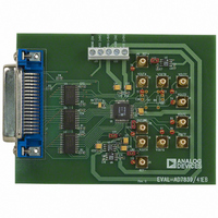
EVAL-AD7841EB Analog Devices Inc, EVAL-AD7841EB Datasheet - Page 10

EVAL-AD7841EB
Manufacturer Part Number
EVAL-AD7841EB
Description
BOARD EVAL FOR AD7841
Manufacturer
Analog Devices Inc
Datasheet
1.EVAL-AD7841EB.pdf
(12 pages)
Specifications of EVAL-AD7841EB
Number Of Dac's
8
Number Of Bits
14
Outputs And Type
8, Single Ended
Sampling Rate (per Second)
32k
Data Interface
Parallel
Settling Time
31µs
Dac Type
Voltage
Voltage Supply Source
Analog and Digital, Dual ±
Operating Temperature
-40°C ~ 85°C
Utilized Ic / Part
AD7841
Lead Free Status / RoHS Status
Contains lead / RoHS non-compliant
AD7841
DUTGND Voltage Range
During power-on, the V
to the relevant DUTGND pins via G
resistor. The DUTGND potential must obey the max ratings at
all times. Thus, the voltage at DUTGND must always be within
the range V
voltages at the V
relevant DUTGND potential during power-on, the voltage
applied to DUTGND should also be kept within the range
GND – 2 V, GND + 2 V.
Once the AD7841 has powered on and the on-chip amplifiers
have settled, any voltage that is now applied to the DUTGND
pin is subtracted from the DAC output, which has been gained
up by a factor of two. Thus, for specified operation, the maximum
voltage that can be applied to the DUTGND pin increases to the
maximum allowable 2 V
age that can be applied to DUTGND is the minimum 2 V
voltage. After the AD7841 has fully powered on, the outputs
can track any DUTGND voltage within this minimum/maxi-
mum range.
Power Supply Sequencing
When operating the AD7841, it is important that ground be
connected at all times to avoid high current states. The recom-
mended power-up sequence is V
can exceed V
absolute maximum ratings section will ensure protection. The
reference inputs and digital inputs should be powered up last.
Should the references exceed V
limiting resistors should be inserted in series with the reference
inputs to limit the current to 20 mA. Logic inputs should not be
applied before V
with the logic inputs should be inserted if these inputs come up
before V
MICROPROCESSOR INTERFACING
Interfacing the AD7841—16-Bit Interface
The AD7841 can be interfaced to a variety of 16-bit micro-
controllers or DSP processors. Figure 10 shows the AD7841
interfaced to a generic 16-bit microcontroller/DSP processor.
The lower address lines from the processor are connected to A0,
A1 and A2 on the AD7841 as shown. The upper address lines
are decoded to provide a chip select signal or an LDAC signal
for the AD7841. The fast interface timing of the AD7841 allows
direct interface to a wide variety of microcontrollers and DSPs
as shown in Figure 10.
CC
.
SS
DD
– 0.3 V, V
OUT
on power-up, the diode scheme shown in the
CC
. Current limiting resistors (470 Ω) in series
pins of the AD7841 stay within ± 2 V of the
DD
OUT
REF
+ 0.3 V. However, in order that the
(+) voltage, and the minimum volt-
pins of the AD7841 are connected
DD
DD
/V
/V
5
SS
SS
and the 14 kΩ thin-film
followed by V
on power-up, current
CC
. If V
REF
CC
(–)
APPLICATIONS
Power Supply Bypassing and Grounding
In any circuit where accuracy is important, careful consideration
of the power supply and ground return layout helps to ensure
the rated performance. The printed circuit board on which the
AD7841 is mounted should be designed such that the analog
and digital sections are separated and confined to certain areas
of the board. This facilitates the use of ground planes that can
be easily separated. A minimum etch technique is generally best
for ground planes as it gives the best shielding. Digital and ana-
log ground planes should be joined at only one place. The GND
pin of the AD7841 should be connected to the AGND of the
system. If the AD7841 is in a system where multiple devices
require an AGND-to-DGND connection, the connection should
be made at one point only, a star ground point that should be
established as close as possible to the AD7841.
Digital lines running under the device should be avoided as
these will couple noise onto the die. The analog ground plane
should be allowed to run under the AD7841 to avoid noise
coupling. The power supply lines of the AD7841 should use as
large a trace as possible to provide low impedance paths and
reduce the effects of glitches on the power supply line. Fast
switching signals like clocks should be shielded with digital
ground to avoid radiating noise to other parts of the board and
should never be run near the analog inputs.
Avoid crossover of digital and analog signals. Traces on opposite
sides of the board should run at right angles to each other. This
reduces the effects of feedthrough through the board. A micro-
strip technique is by far the best but not always possible with a
double sided board. In this technique, the component side of
the board is dedicated to ground plane while signal traces are
placed on the solder side.
DSP PROCESSOR
CONTROLLER/
UPPER BITS OF
ADDRESS BUS
DATA
BUS
R/W
D13
ADDITIONAL PINS OMITTED FOR CLARITY
D0
A2
A1
A0
ADDRESS
DECODE
D13
A2
A1
A0
WR
D0
CS
LDAC
AD7841


