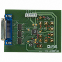
EVAL-AD7841EB Analog Devices Inc, EVAL-AD7841EB Datasheet - Page 9

EVAL-AD7841EB
Manufacturer Part Number
EVAL-AD7841EB
Description
BOARD EVAL FOR AD7841
Manufacturer
Analog Devices Inc
Datasheet
1.EVAL-AD7841EB.pdf
(12 pages)
Specifications of EVAL-AD7841EB
Number Of Dac's
8
Number Of Bits
14
Outputs And Type
8, Single Ended
Sampling Rate (per Second)
32k
Data Interface
Parallel
Settling Time
31µs
Dac Type
Voltage
Voltage Supply Source
Analog and Digital, Dual ±
Operating Temperature
-40°C ~ 85°C
Utilized Ic / Part
AD7841
Lead Free Status / RoHS Status
Contains lead / RoHS non-compliant
Power-On with CLR Low
The output stage of the AD7841 has been designed to allow
output stability during power-on. If CLR is kept low during
power-on, then just after power is applied to the AD7841, the
situation is as depicted in Figure 5. G
while G
V
G
parallel with the gain resistors of the output amplifier. The
output amplifier is connected as a unity gain buffer via G
the DUTGND voltage is applied to the buffer input via G
amplifier’s output is thus at the same voltage as the DUTGND
pin. The output stage remains configured as in Figure 5 until
the voltage at V
–3 V. By now the output amplifier has enough headroom to
handle signals at its input and has also had time to settle. The
internal power-on circuitry opens G
G
fier is configured in its noise gain configuration via G
The DUTGND voltage is still connected to the noninverting
input via G
V
opening of G
via the configuration shown in Figure 6.
When CLR is taken back high, the output stage is configured as
shown in Figure 7. The internal control logic closes G
opens G
gain-of-two configuration. The voltage that appears on the V
pins is determined by the data present in the DAC registers.
OUT
OUT
5
6
. This situation is shown in Figure 6. Now the output ampli-
and a 14 kΩ resistor. This thin-film resistor is connected in
is kept within a few hundred millivolts of DUTGND via
has been disconnected from the DUTGND pin by the
2
DAC
DAC
2
, G
. The output amr})fier is connected in a noninverting
2
3
and this voltage appears at V
5
and G
, but will track the voltage present at DUTGND
DD
G
G
G
G
1
1
2
2
5
exceeds 7 V and V
are closed.
DUTGND
DUTGND
R
R
G
G
4
4
G
G
G
G
3
5
3
5
R
R
3
14k
14k
and G
1
, G
SS
G
G
6
is more negative than
OUT
6
4
and G
5
and closes G
.
6
are open
4
V
V
OUT
and G
OUT
2
. The
1
3
CLR
, and
4
and
CLR
and
OUT
6
.
Power-On with CLR High
If CLR is high on the application of power to the device, the
output stages of the AD7841 are configured as in Figure 8 while
V
closed and G
DAC to the input of its output amplifier. G
while G
a unity gain buffer. V
through a 14 kΩ resistor until V
negative than –3 V.
When the difference between the supply voltages reaches 10 V,
the internal power-on circuitry opens G
and G
DD
is less than 7 V and V
6
4
configuring the output stage as shown in Figure 9.
DAC
DAC
DAC
and G
2
is open, thereby connecting the output of the
6
are open, thus connecting the output amplifier as
G
G
G
G
G
G
1
1
1
2
2
2
OUT
DUTGND
DUTGND
DUTGND
R
R
R
is connected to DUTGND via G
G
G
SS
G
4
4
4
is more positive than –3 V. G
DD
G
G
G
G
G
G
3
5
3
5
3
5
exceeds 7 V and V
R
R
R
14k
14k
14k
CLR
3
G
G
G
and G
6
6
6
3
and G
5
AD7841
CLR
CLR
and closes G
5
are closed
V
V
V
SS
OUT
OUT
OUT
is more
1
5
4
is


