EVAL-AD7841EB Analog Devices Inc, EVAL-AD7841EB Datasheet - Page 3
EVAL-AD7841EB
Manufacturer Part Number
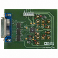
EVAL-AD7841EB
Description
BOARD EVAL FOR AD7841
Manufacturer
Analog Devices Inc
Datasheet
1.EVAL-AD7841EB.pdf
(12 pages)
Specifications of EVAL-AD7841EB
Number Of Dac's
8
Number Of Bits
14
Outputs And Type
8, Single Ended
Sampling Rate (per Second)
32k
Data Interface
Parallel
Settling Time
31µs
Dac Type
Voltage
Voltage Supply Source
Analog and Digital, Dual ±
Operating Temperature
-40°C ~ 85°C
Utilized Ic / Part
AD7841
Lead Free Status / RoHS Status
Contains lead / RoHS non-compliant


Parameter
DYNAMIC PERFORMANCE
Specifications subject to change without notice.
AC PERFORMANCE CHARACTERISTICS
TIMING SPECIFICATIONS
Parameter
t
t
t
t
t
t
t
t
t
t
t
NOTES
1
2
Specifications subject to change without notice.
1
2
3
4
5
6
7
8
9
10
11
All input signals are specified with tr = tf = 5 ns (10% to 90% of 5 V) and timed from a voltage level of 1.6 V.
Rise and fall times should be no longer than 50 ns.
Output Voltage Settling Time
Slew Rate
Digital-to-Analog Glitch Impulse 230
Channel-to-Channel Isolation
DAC-to-DAC Crosstalk
Digital Crosstalk
Digital Feedthrough
Output Noise Spectral Density
@ 1 kHz
A0, A1, A2
Limit at T
15
0
50
50
0
0
20
0
31
300
50
DATA
LDAC
V
V
CLR
WR
OUT
OUT
CS
MIN,
A & B
Versions
31
0.7
99
40
0.2
0.1
200
1, 2
t
t
1
5
T
MAX
(V
t
t
3
4
t
CC
7
t
10
= 5 V
t
t
Unit
µs typ
V/µs typ
nV-s typ
dB typ
nV-s typ
nV-s typ
nV-s typ
nV/√Hz typ
t
6
2
8
t
9
5%; V
(These characteristics are included for Design Guidance and are not subject
to production testing.)
DD
= 15 V
Unit
ns min
ns min
ns min
ns min
ns min
ns min
ns min
ns min
µs typ
ns max
ns min
Test Conditions/Comments
Full-Scale Change to ± 1/2 LSB. DAC Latch Contents Alternately
Loaded with All 0s and All 1s
Measured with V
Alternately Loaded with 1FFF Hex and 2000 Hex. Not Dependent
on Load Conditions
See Terminology
See Terminology
Feedthrough to DAC Output Under Test Due to Change in Digital
Input Code to Another Converter
Effect of Input Bus Activity on DAC Output Under Test
All 1s Loaded to DAC. V
10%; V
SS
= –15 V
REF
(+) = +5 V, V
t
REF
11
10%; GND = DUTGND = 0 V)
(+) = V
Description
Address to WR Setup Time
Address to WR Hold Time
CS Pulsewidth Low
WR Pulsewidth Low
CS to WR Setup Time
WR to CS Hold Time
Data Setup Time
Data Hold Time
Settling Time
CLR Pulse Activation Time
LDAC Pulsewidth Low
REF
REF
(–) = –5 V. DAC Latch
(–) = 0 V
AD7841
Related parts for EVAL-AD7841EB
Image
Part Number
Description
Manufacturer
Datasheet
Request
R

Part Number:
Description:
ENERCHIP CC EVAL KIT
Manufacturer:
Cymbet Corporation
Datasheet:

Part Number:
Description:
BOARD EVAL FOR AD976
Manufacturer:
Analog Devices Inc
Datasheet:

Part Number:
Description:
BOARD EVAL FOR ADXL345
Manufacturer:
Analog Devices Inc
Datasheet:

Part Number:
Description:
ENERCHIP CC SEH EVAL KIT
Manufacturer:
Cymbet Corporation
Datasheet:

Part Number:
Description:
ENERCHIP EP ENERGY HARVEST EVAL
Manufacturer:
Cymbet Corporation
Datasheet:

Part Number:
Description:
EVAL BOARD FOR TW6864-LB2-GR
Manufacturer:
Intersil
Datasheet:
Part Number:
Description:
EVAL BOARD FOR TW8816-LB3-GR
Manufacturer:
Intersil
Datasheet:
Part Number:
Description:
EVAL BOARD FOR TW8817-TA3-GRS
Manufacturer:
Intersil
Datasheet:

Part Number:
Description:
EVALUATION MODULE FOR ADUM4160
Manufacturer:
Analog Devices Inc
Datasheet:

Part Number:
Description:
BOARD EVALUATION ADCMP581BCP
Manufacturer:
Analog Devices Inc
Datasheet:
Part Number:
Description:
BOARD EVALUATION ADM1041
Manufacturer:
Analog Devices Inc
Datasheet:

Part Number:
Description:
EVAL BOARD FOR STM32F107VCT
Manufacturer:
STMicroelectronics
Datasheet:
Part Number:
Description:
BOARD EVAL FOR AD1954
Manufacturer:
Analog Devices Inc
Datasheet:
Part Number:
Description:
BOARD EVAL FOR AD1955
Manufacturer:
Analog Devices Inc
Datasheet:

Part Number:
Description:
BOARD EVAL FOR AD7655
Manufacturer:
Analog Devices Inc
Datasheet: