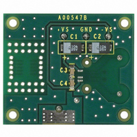
AD8221-EVAL Analog Devices Inc, AD8221-EVAL Datasheet - Page 18

AD8221-EVAL
Manufacturer Part Number
AD8221-EVAL
Description
BOARD EVAL FOR AD8221
Manufacturer
Analog Devices Inc
Datasheet
1.AD8221-EVAL.pdf
(24 pages)
Specifications of AD8221-EVAL
Design Resources
Low Cost, High Voltage, Programmable Gain Instrumentation Amplifier Using AD5292 and AD8221 (CN0114) Low Cost Programmable Gain Instrumentation Amplifier Circuit Using ADG1611 and AD620 (CN0146)
Module/board Type
Evaluation Board
For Use With/related Products
AD8221
Lead Free Status / RoHS Status
Contains lead / RoHS non-compliant
Other names
Q1815689
AD8221
GAIN SELECTION
Placing a resistor across the R
AD8221, which can be calculated by referring to Table 6 or
by using the gain equation.
Table 6. Gains Achieved Using 1% Resistors
1% Standard Table Value of R
49.9 k
12.4 k
5.49 k
2.61 k
1.00 k
499
249
100
49.9
The AD8221 defaults to G = 1 when no gain resistor is used.
Gain accuracy is determined by the absolute tolerance of R
The TC of the external gain resistor increases the gain drift of
the instrumentation amplifier. Gain error and gain drift are kept
to a minimum when the gain resistor is not used.
LAYOUT
Careful board layout maximizes system performance. Traces
from the gain setting resistor to the R
short as possible to minimize parasitic inductance. To ensure
the most accurate output, the trace from the REF pin should
either be connected to the local ground of the AD8221, as shown
in Figure 47, or connected to a voltage that is referenced to the
local ground of the AD8221.
Common-Mode Rejection
One benefit of the high CMRR over frequency of the AD8221 is
that it has greater immunity to disturbances, such as line noise
and its associated harmonics, than do typical instrumentation
amplifiers. Typically, these amplifiers have CMRR fall-off at
200 Hz; common-mode filters are often used to compensate for
this shortcoming. The AD8221 is able to reject CMRR over a
greater frequency range, reducing the need for filtering.
A well implemented layout helps to maintain the high CMRR
over frequency of the AD8221. Input source impedance and
capacitance should be closely matched. In addition, source
resistance and capacitance should be placed as close to the
inputs as permissible.
R
G
=
49
G
4 .
−
kΩ
1
G
G
terminals set the gain of
(Ω)
G
pins should be kept as
Calculated Gain
1.990
4.984
9.998
19.93
50.40
100.0
199.4
495.0
991.0
G
.
Rev. C | Page 18 of 24
Grounding
The output voltage of the AD8221 is developed with respect to
the potential on the reference terminal. Care should be taken to
tie REF to the appropriate local ground.
In mixed-signal environments, low level analog signals need to
be isolated from the noisy digital environment. Many ADCs
have separate analog and digital ground pins. Although it is
convenient to tie both grounds to a single ground plane, the
current traveling through the ground wires and PC board may
cause hundreds of millivolts of error. Therefore, separate analog
and digital ground returns should be used to minimize the
current flow from sensitive points to the system ground. An
example layout is shown in Figure 45 and Figure 46.
Figure 46. Bottom Layer of the AD8221-EVAL
Figure 45. Top Layer of the AD8221-EVAL


