AD8221-EVAL Analog Devices Inc, AD8221-EVAL Datasheet - Page 19
AD8221-EVAL
Manufacturer Part Number
AD8221-EVAL
Description
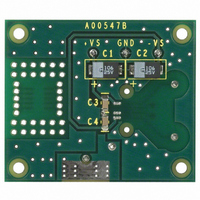
BOARD EVAL FOR AD8221
Manufacturer
Analog Devices Inc
Datasheet
1.AD8221-EVAL.pdf
(24 pages)
Specifications of AD8221-EVAL
Design Resources
Low Cost, High Voltage, Programmable Gain Instrumentation Amplifier Using AD5292 and AD8221 (CN0114) Low Cost Programmable Gain Instrumentation Amplifier Circuit Using ADG1611 and AD620 (CN0146)
Module/board Type
Evaluation Board
For Use With/related Products
AD8221
Lead Free Status / RoHS Status
Contains lead / RoHS non-compliant
Other names
Q1815689


REFERENCE TERMINAL
As shown in Figure 43, the reference terminal, REF, is at one
end of a 10 kΩ resistor. The output of the instrumentation
amplifier is referenced to the voltage on the REF terminal; this
is useful when the output signal needs to be offset to a precise
midsupply level. For example, a voltage source can be tied to the
REF pin to level-shift the output so that the AD8221 can interface
with an ADC. The allowable reference voltage range is a function
of the gain, input, and supply voltage. The REF pin should not
exceed either +V
For best performance, source impedance to the REF terminal
should be kept low, because parasitic resistance can adversely
affect CMRR and gain accuracy.
POWER SUPPLY REGULATION AND BYPASSING
A stable dc voltage should be used to power the instrumentation
amplifier. Noise on the supply pins can adversely affect
performance. Bypass capacitors should be used to decouple
the amplifier.
A 0.1 µF capacitor should be placed close to each supply pin.
As shown in Figure 47, a 10 µF tantalum capacitor can be used
further away from the part. In most cases, it can be shared by
other precision integrated circuits.
INPUT BIAS CURRENT RETURN PATH
The input bias current of the AD8221 must have a return path
to common. When the source, such as a thermocouple, cannot
provide a return current path, one should be created, as shown
in Figure 48.
Figure 47. Supply Decoupling, REF, and Output Referred to Local Ground
S
or –V
+IN
–IN
S
by more than 0.5 V.
AD8221
+V
–V
S
S
0.1µF
0.1µF
REF
10µF
10µF
LOAD
V
OUT
Rev. C | Page 19 of 24
INPUT PROTECTION
All terminals of the AD8221 are protected against ESD, 1 kV
Human Body Model. In addition, the input structure allows for
dc overload conditions below the negative supply, −V
internal 400 Ω resistors limit current in the event of a negative
fault condition. However, in the case of a dc overload voltage
above the positive supply, +V
through the ESD diode to the positive rail. Therefore, an external
resistor should be used in series with the input to limit current
for voltages above +Vs. In either scenario, the AD8221 can
safely handle a continuous 6 mA current, I = V
positive overvoltage and I = V
overvoltage.
For applications where the AD8221 encounters extreme
overload voltages, as in cardiac defibrillators, external series
resistors, and low leakage diode clamps, such as BAV199Ls,
FJH1100s, or SP720s should be used.
f
HIGH-PASS
Figure 48. Creating an I
=
2πRC
1
TRANSFORMER
THERMOCOUPLE
C
C
CAPACITOR COUPLED
S
, a large current flows directly
IN
R
R
/(400 Ω + R
AD8221
AD8221
AD8221
BIAS
+V
+V
–V
+V
–V
–V
S
S
S
S
S
S
Path
EXT
) for negative
REF
REF
REF
IN
/R
EXT
AD8221
S
. The
for
Related parts for AD8221-EVAL
Image
Part Number
Description
Manufacturer
Datasheet
Request
R

Part Number:
Description:
AD8221/6/8/9 SO Pkg Eval Bd
Manufacturer:
Analog Devices Inc
Datasheet:

Part Number:
Description:
±1.7g Dual-Axis IMEMS Accelerometer Evaluation Board
Manufacturer:
Analog Devices Inc
Datasheet:
Part Number:
Description:
Inertial Sensor Evaluation System
Manufacturer:
Analog Devices Inc
Datasheet:
Part Number:
Description:
Manufacturer:
Analog Devices Inc
Datasheet:
Part Number:
Description:
Manufacturer:
Analog Devices Inc
Datasheet:
Part Number:
Description:
Manufacturer:
Analog Devices Inc
Datasheet:
Part Number:
Description:
Manufacturer:
Analog Devices Inc
Datasheet:
Part Number:
Description:
Manufacturer:
Analog Devices Inc
Datasheet:
Part Number:
Description:
Manufacturer:
Analog Devices Inc
Datasheet:
Part Number:
Description:
Manufacturer:
Analog Devices Inc
Datasheet:
Part Number:
Description:
Manufacturer:
Analog Devices Inc
Datasheet:
Part Number:
Description:
Manufacturer:
Analog Devices Inc
Datasheet:
Part Number:
Description:
Manufacturer:
Analog Devices Inc
Datasheet: