AD8221-EVAL Analog Devices Inc, AD8221-EVAL Datasheet - Page 20
AD8221-EVAL
Manufacturer Part Number
AD8221-EVAL
Description
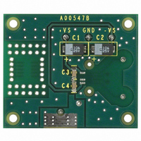
BOARD EVAL FOR AD8221
Manufacturer
Analog Devices Inc
Datasheet
1.AD8221-EVAL.pdf
(24 pages)
Specifications of AD8221-EVAL
Design Resources
Low Cost, High Voltage, Programmable Gain Instrumentation Amplifier Using AD5292 and AD8221 (CN0114) Low Cost Programmable Gain Instrumentation Amplifier Circuit Using ADG1611 and AD620 (CN0146)
Module/board Type
Evaluation Board
For Use With/related Products
AD8221
Lead Free Status / RoHS Status
Contains lead / RoHS non-compliant
Other names
Q1815689


AD8221
RF INTERFERENCE
RF rectification is often a problem when amplifiers are used in
applications where there are strong RF signals. The disturbance
can appear as a small dc offset voltage. High frequency signals
can be filtered with a low-pass RC network placed at the input
of the instrumentation amplifier, as shown in Figure 49. The
filter limits the input signal bandwidth according to the following
relationship:
where C
10µF
10µF
FilterFreq
FilterFreq
D
≥ 10C
0.1µF
0.1µF
4.02kΩ
4.02kΩ
R
R
Diff
CM
C
C
C
C
.
+IN
–IN
C
D
C
=
=
π 2
π 2
Figure 49. RFI Suppression
AD8221
1nF
10nF
1nF
+12V
–12V
RC
R
1
2 (
C
499Ω
C
1
R1
D
0.1µF
0.1µF
REF
+
+IN
–IN
C
C
10kΩ
10kΩ
)
AD8221
+15V
–15V
R1
R2
+2.5V
REF
+12V
–12V
OP27
10µF
10µF
0.1µF
0.1µF
V
Figure 51. Interfacing to a Differential Input ADC
OUT
1kΩ
R3
Rev. C | Page 20 of 24
1kΩ
R4
499Ω
R5
470pF
C1
C
mode signal. Values of R and C
RFI. Mismatch between the R × C
R × C
By using a value of C
of the mismatch is reduced, and therefore, performance is
improved.
PRECISION STRAIN GAGE
The low offset and high CMRR over frequency of the AD8221
make it an excellent candidate for bridge measurements. As
shown in Figure 50, the bridge can be directly connected to
the inputs of the amplifier.
CONDITIONING ±10 V SIGNALS FOR A +5 V
DIFFERENTIAL INPUT ADC
There is a need in many applications to condition ±10 V signals.
However, many of today’s ADCs and digital ICs operate on
much lower, single-supply voltages. Furthermore, new ADCs
have differential inputs because they provide better common-
mode rejection, noise immunity, and performance at low supply
voltages. Interfacing a ±10 V, single-ended instrumentation
amplifier to a +5 V, differential ADC can be a challenge.
Interfacing the instrumentation amplifier to the ADC requires
attenuation and a level shift. A solution is shown in Figure 51.
D
affects the difference signal, and C
+12V
–12V
+12V
–12V
AD8022
AD8022
350Ω
350Ω
(½)
(½)
C
at the negative input degrades the CMRR of the AD8221.
0.1µF
0.1µF
0.1µF
0.1µF
350Ω
350Ω
27.4Ω
Figure 50. Precision Strain Gage
27.4Ω
R6
R7
220µF
+5V
D
one magnitude larger than C
C2
220nF
10µF
10µF
0.1µF
C
10nF
should be chosen to minimize
C
0.1µF
at the positive input and the
VIN(+)
VIN(–)
C
R
AGND DGND REF1 REF2
affects the common-
+V
+IN
–IN
IN
AD780
+5V
AV
AD7723
+5V
GND
10nF
DD
+
–
AD8221
V
OUT
C
22µF
2.5V
+5V
, the effect
+2.5V
DV
DD
Related parts for AD8221-EVAL
Image
Part Number
Description
Manufacturer
Datasheet
Request
R

Part Number:
Description:
AD8221/6/8/9 SO Pkg Eval Bd
Manufacturer:
Analog Devices Inc
Datasheet:

Part Number:
Description:
±1.7g Dual-Axis IMEMS Accelerometer Evaluation Board
Manufacturer:
Analog Devices Inc
Datasheet:
Part Number:
Description:
Inertial Sensor Evaluation System
Manufacturer:
Analog Devices Inc
Datasheet:
Part Number:
Description:
Manufacturer:
Analog Devices Inc
Datasheet:
Part Number:
Description:
Manufacturer:
Analog Devices Inc
Datasheet:
Part Number:
Description:
Manufacturer:
Analog Devices Inc
Datasheet:
Part Number:
Description:
Manufacturer:
Analog Devices Inc
Datasheet:
Part Number:
Description:
Manufacturer:
Analog Devices Inc
Datasheet:
Part Number:
Description:
Manufacturer:
Analog Devices Inc
Datasheet:
Part Number:
Description:
Manufacturer:
Analog Devices Inc
Datasheet:
Part Number:
Description:
Manufacturer:
Analog Devices Inc
Datasheet:
Part Number:
Description:
Manufacturer:
Analog Devices Inc
Datasheet:
Part Number:
Description:
Manufacturer:
Analog Devices Inc
Datasheet: