AD8221-EVAL Analog Devices Inc, AD8221-EVAL Datasheet - Page 22
AD8221-EVAL
Manufacturer Part Number
AD8221-EVAL
Description
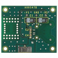
BOARD EVAL FOR AD8221
Manufacturer
Analog Devices Inc
Datasheet
1.AD8221-EVAL.pdf
(24 pages)
Specifications of AD8221-EVAL
Design Resources
Low Cost, High Voltage, Programmable Gain Instrumentation Amplifier Using AD5292 and AD8221 (CN0114) Low Cost Programmable Gain Instrumentation Amplifier Circuit Using ADG1611 and AD620 (CN0146)
Module/board Type
Evaluation Board
For Use With/related Products
AD8221
Lead Free Status / RoHS Status
Contains lead / RoHS non-compliant
Other names
Q1815689


AD8221
DIE INFORMATION
Die size: 1575 μm × 2230 μm
Die thickness: 381 μm
To minimize gain errors introduced by the bond wires, use Kelvin connections between the chip and the gain resistor, R
Pad 2A and Pad 2B in parallel to one end of R
where R
Table 7. Bond Pad Information
Pad No.
1
2A
2B
3A
3B
4
5
6
7
8
1
The pad coordinates indicate the center of each pad, referenced to the center of the die. The die orientation is indicated by the logo, as shown in Figure 53.
G
is not required, Pad 2A and Pad 2B must be bonded together as well as the Pad 3A and Pad 3B.
Mnemonic
−IN
R
R
R
R
+IN
−V
REF
V
+V
G
G
G
G
OUT
S
S
X (μm)
–379
–446
–615
–619
–490
–621
+635
+649
+612
+636
G
and Pad 3A and Pad 3B in parallel to the other end of R
LOGO
Figure 53. Bond Pad Diagram
Rev. C | Page 22 of 24
3A
2B
4
3B
2A
1
7
5
8
6
Pad Coordinates
Y (μm)
+951
+826
+474
+211
–190
–622
–823
–339
+84
+570
1
G
. For unity gain applications
G
, by connecting
Related parts for AD8221-EVAL
Image
Part Number
Description
Manufacturer
Datasheet
Request
R

Part Number:
Description:
AD8221/6/8/9 SO Pkg Eval Bd
Manufacturer:
Analog Devices Inc
Datasheet:

Part Number:
Description:
±1.7g Dual-Axis IMEMS Accelerometer Evaluation Board
Manufacturer:
Analog Devices Inc
Datasheet:
Part Number:
Description:
Inertial Sensor Evaluation System
Manufacturer:
Analog Devices Inc
Datasheet:
Part Number:
Description:
Manufacturer:
Analog Devices Inc
Datasheet:
Part Number:
Description:
Manufacturer:
Analog Devices Inc
Datasheet:
Part Number:
Description:
Manufacturer:
Analog Devices Inc
Datasheet:
Part Number:
Description:
Manufacturer:
Analog Devices Inc
Datasheet:
Part Number:
Description:
Manufacturer:
Analog Devices Inc
Datasheet:
Part Number:
Description:
Manufacturer:
Analog Devices Inc
Datasheet:
Part Number:
Description:
Manufacturer:
Analog Devices Inc
Datasheet:
Part Number:
Description:
Manufacturer:
Analog Devices Inc
Datasheet:
Part Number:
Description:
Manufacturer:
Analog Devices Inc
Datasheet:
Part Number:
Description:
Manufacturer:
Analog Devices Inc
Datasheet: