DK-SI-2SGX90N Altera, DK-SI-2SGX90N Datasheet - Page 11
DK-SI-2SGX90N
Manufacturer Part Number
DK-SI-2SGX90N
Description
SI KIT W/SII GX EP2SGX90N
Manufacturer
Altera
Series
Stratix® IIr
Type
DSPr
Datasheet
1.DK-SI-2SGX90N.pdf
(38 pages)
Specifications of DK-SI-2SGX90N
Contents
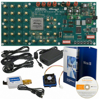
Dev Board, Quartus®II Web Edition, Cables, Accessories, Reference Designs and Demos
For Use With/related Products
Stratix ll GX 2SGX90N
Lead Free Status / RoHS Status
Lead free / RoHS Compliant
Other names
544-1724
Available stocks
Company
Part Number
Manufacturer
Quantity
Price


Figure 2–1. Stratix II GX Transceiver Signal Integrity Development Board
Altera Corporation
June 2006
SMA Output Clock Connectors
SMA Output Clock Connectors
Transceivers (J7, J8)
Transceivers (J9, J10)
Reference Clock for Quad 1
Reference Clock for Quad 3
Receive Connectors
(J26 through J49)
SMA Transmit &
Stratix II GX Device (U20)
f
Temperature Sensor
with Alarm (U17)
Configuration
Done LED (D14)
156.25-MHz
Oscillator (U9)
Figure 2–1
development board.
Refer to the Stratix II GX EP2SGX90 Transceiver Signal Integrity
Development Board Reference Manual (available on the Transceiver SI
Development Kit, Stratix II GX Edition CD-ROM) for information on the
board’s components.
Hardware Requirements
All of the hardware that you need to use the board is provided with the
Transceiver Signal Integrity Development Kit, Stratix II GX Edition.
Buffer (U8)
Differential
Fan-out
Used for System Clock (U10)
50-MHz Oscillator
Transceiver Signal Integrity Development Kit, Stratix II GX Edition
shows the Stratix II GX EP2SGX90 transceiver signal integrity
Clock
Generator (U5)
Getting Started User Guide
Connection Jacks (J15, J17-21)
25-MHz
Crystal (U6)
Differential to
Single-Ended
Buffer (U7)
Switch (S9)
Optional Power Input
Slide
EPCS64 Device (U22)
Debug
Header (J1)
Clock
Setting
DIP Switch
Bank (S8)
User LEDs
(D1 through D8)
VCCH Voltage (J50)
Jumper Header for
User Push-Button
Switches (S1 through S6)
Connectors for FPGA (J12, J14)
SMA Input Clock
User DIP Switch
Bank (S7)
10-pin Configuration Header
10-pin JTAG Configuration
Header for FPGA (J24)
for EPCS64 Device (J23)
Power Switch (S10)
Displays (D9, D10)
USB Interface (U2)
Dual 7-Segment
16 Mbytes Flash
Memory (U19)
Power LED (D13)
Power Supply Input
USB Connector (J2)
Getting Started
2–3
Related parts for DK-SI-2SGX90N
Image
Part Number
Description
Manufacturer
Datasheet
Request
R

Part Number:
Description:
KIT DEV STRATIX IV 4SGX230N/C2
Manufacturer:
Altera
Datasheet:

Part Number:
Description:
KIT DEV STRATIX IV TRANSCEIVER
Manufacturer:
Altera
Datasheet:

Part Number:
Description:
KIT DEV STRATIX V FPGA 5SGXEA7
Manufacturer:
Altera
Datasheet:

Part Number:
Description:
Programmable Logic IC Development Tools FPGA Starter Kit For Stratix V 5SGXEA7
Manufacturer:
Altera Corporation
Part Number:
Description:
Programmable Logic IC Development Tools FPGA Starter Kit For Stratix V 5SGTMC7
Manufacturer:
Altera Corporation
Part Number:
Description:
Programmable Logic IC Development Tools FPGA Starter Kit For Stratix V 5SGTMC7 ES
Manufacturer:
Altera Corporation

Part Number:
Description:
CYCLONE II STARTER KIT EP2C20N
Manufacturer:
Altera
Datasheet:
Part Number:
Description:
CPLD, EP610 Family, ECMOS Process, 300 Gates, 16 Macro Cells, 16 Reg., 16 User I/Os, 5V Supply, 35 Speed Grade, 24DIP
Manufacturer:
Altera Corporation
Datasheet:
Part Number:
Description:
CPLD, EP610 Family, ECMOS Process, 300 Gates, 16 Macro Cells, 16 Reg., 16 User I/Os, 5V Supply, 15 Speed Grade, 24DIP
Manufacturer:
Altera Corporation
Datasheet:
Part Number:
Description:
Manufacturer:
Altera Corporation
Datasheet:
Part Number:
Description:
CPLD, EP610 Family, ECMOS Process, 300 Gates, 16 Macro Cells, 16 Reg., 16 User I/Os, 5V Supply, 30 Speed Grade, 24DIP
Manufacturer:
Altera Corporation
Datasheet:
Part Number:
Description:
High-performance, low-power erasable programmable logic devices with 8 macrocells, 10ns
Manufacturer:
Altera Corporation
Datasheet:
Part Number:
Description:
High-performance, low-power erasable programmable logic devices with 8 macrocells, 7ns
Manufacturer:
Altera Corporation
Datasheet: