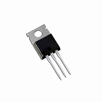
IRFZ34E International Rectifier, IRFZ34E Datasheet
IRFZ34E
Specifications of IRFZ34E
Available stocks


Related parts for IRFZ34E

IRFZ34E Summary of contents
Page 1
... Storage Temperature Range STG Soldering Temperature, for 10 seconds Mounting torque, 6- srew Thermal Resistance R Junction-to-Case JC R Case-to-Sink, Flat, Greased Surface CS R Junction-to-Ambient JA G Parameter @ 10V GS @ 10V GS Parameter PD - 9.1672A IRFZ34E ® HEXFET Power MOSFET 60V DSS R = 0.042 DS(on 28A D S TO-220AB Max 112 68 0.46 ± ...
Page 2
... IRFZ34E Electrical Characteristics @ T Parameter V Drain-to-Source Breakdown Voltage (BR)DSS Breakdown Voltage Temp. Coefficient (BR)DSS J R Static Drain-to-Source On-Resistance DS(ON) V Gate Threshold Voltage GS(th) g Forward Transconductance fs I Drain-to-Source Leakage Current DSS Gate-to-Source Forward Leakage I GSS Gate-to-Source Reverse Leakage Q Total Gate Charge g Q Gate-to-Source Charge ...
Page 3
... V , Gate-to-Source Voltage (V) GS Fig 3. Typical Transfer Characteristics 4.5V ° 100 ° 175 25V DS 20µs PULSE WIDTH IRFZ34E 1000 VGS TOP 15V 10V 8.0V 7.0V 6.0V 5.5V 100 5.0V BOTTOM 4. 20µs PULSE WIDTH T = 175 C 0.1 0 Drain-to-Source Voltage (V) DS Fig 2. Typical Output Characteristics 2 ...
Page 4
... IRFZ34E 1200 iss rss gd 1000 oss ds C iss 800 600 C oss 400 C rss 200 Drain-to-Source Voltage (V) DS Fig 5. Typical Capacitance Vs. Drain-to-Source Voltage 1000 100 ° 150 0.1 0.2 0.6 1.0 V ,Source-to-Drain Voltage (V) SD Fig 7. Typical Source-Drain Diode Forward Voltage f = 1MHz ...
Page 5
... RESPONSE) 0.01 0.00001 0.0001 Fig 11. Maximum Effective Transient Thermal Impedance, Junction-to-Case Fig 10a. Switching Time Test Circuit V 90% 125 150 175 ° 10% V Fig 10b. Switching Time Waveforms 0.001 t , Rectangular Pulse Duration (sec) 1 IRFZ34E D.U. Pulse Width µs Duty Factor ...
Page 6
... IRFZ34E Fig 12a. Unclamped Inductive Test Circuit Fig 12b. Unclamped Inductive Waveforms Charge Fig 13a. Basic Gate Charge Waveform L D.U. 0.01 V (BR)DSS V DD 200 150 100 100 Starting T , Junction Temperature ( C) J Fig 12c. Maximum Avalanche Energy Vs. Drain Current Current Regulator Same Type as D.U.T. ...
Page 7
... Fig 14. For N-Channel HEXFETS Circuit Layout Considerations Low Stray Inductance Ground Plane Low Leakage Inductance Current Transformer - + dv/dt controlled Driver same type as D.U.T. I controlled by Duty Factor "D" SD D.U.T. - Device Under Test P. Period Current di/dt Diode Recovery dv/dt Forward Drop 5% IRFZ34E + =10V * ...
Page 8
... IRFZ34E Package Outline TO-220AB Outline Dimensions are shown in millimeters (inches) 10 10 .87 (. .62 (. 5.24 (. 4.84 (. .09 (. .47 (. .40 (. . & 14 82 LING SIO N : INC H Part Marking Information TO-220AB ITH WORLD HEADQUARTERS: 233 Kansas St., El Segundo, California 90245, Tel: (310) 322 3331 EUROPEAN HEADQUARTERS: Hurst Green, Oxted, Surrey RH8 9BB, UK Tel 1883 732020 IR CANADA: 7321 Victoria Park Ave., Suite 201, Markham, Ontario L3R 2Z8, Tel: (905) 475 1897 IR FAR EAST: K& ...