ATTINY461-20MU Atmel, ATTINY461-20MU Datasheet - Page 180
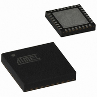
ATTINY461-20MU
Manufacturer Part Number
ATTINY461-20MU
Description
IC AVR MCU 4K 20MHZ 32-QFN
Manufacturer
Atmel
Series
AVR® ATtinyr
Specifications of ATTINY461-20MU
Core Processor
AVR
Core Size
8-Bit
Speed
20MHz
Connectivity
USI
Peripherals
Brown-out Detect/Reset, POR, PWM, WDT
Number Of I /o
16
Program Memory Size
4KB (2K x 16)
Program Memory Type
FLASH
Eeprom Size
256 x 8
Ram Size
256 x 8
Voltage - Supply (vcc/vdd)
2.7 V ~ 5.5 V
Data Converters
A/D 11x10b
Oscillator Type
Internal
Operating Temperature
-40°C ~ 85°C
Package / Case
32-VQFN Exposed Pad, 32-HVQFN, 32-SQFN, 32-DHVQFN
Processor Series
ATTINY4x
Core
AVR8
Data Bus Width
8 bit
Data Ram Size
256 B
Interface Type
2-Wire, SPI, USI
Maximum Clock Frequency
20 MHz
Number Of Programmable I/os
16
Number Of Timers
2
Maximum Operating Temperature
+ 85 C
Mounting Style
SMD/SMT
3rd Party Development Tools
EWAVR, EWAVR-BL
Development Tools By Supplier
ATAVRDRAGON, ATSTK500, ATSTK600, ATAVRISP2, ATAVRONEKIT
Minimum Operating Temperature
- 40 C
On-chip Adc
10 bit, 11 Channel
For Use With
ATSTK600-DIP40 - STK600 SOCKET/ADAPTER 40-PDIPATAVRBC100 - REF DESIGN KIT BATTERY CHARGER770-1007 - ISP 4PORT ATMEL AVR MCU SPI/JTAG
Lead Free Status / RoHS Status
Lead free / RoHS Compliant
Available stocks
Company
Part Number
Manufacturer
Quantity
Price
Company:

Part Number:
ATTINY461-20MU
Manufacturer:
KODENSHI
Quantity:
991
Company:
Part Number:
ATTINY461-20MUR
Manufacturer:
ATMEL
Quantity:
5 560


18.7.3
18.7.4
18.7.5
180
ATtiny261/461/861
Considerations for Efficient Programming
Chip Erase
Programming the Flash
The loaded command and address are retained in the device during programming. For efficient
programming, the following should be considered:
The Chip Erase will erase the Flash and EEPROM memories plus lock bits. The Lock bits are
not reset until the program memory has been completely erased. The Fuse bits are not
changed. A Chip Erase must be performed before the Flash and/or EEPROM are
reprogrammed.
Note:
The Flash is organized in pages, see
the program data is latched into a page buffer. This allows one page of program data to be pro-
grammed simultaneously. The following procedure describes how to program the entire Flash
memory (see
• The command needs only be loaded once when writing or reading multiple memory
• Skip writing the data value 0xFF, that is the contents of the entire EEPROM (unless the
• Address high byte needs only be loaded before programming or reading a new 256 word
1. Load Command “Chip Erase”:
1. Load Command “Write Flash”:
2. Load Address Low byte:
locations.
EESAVE Fuse is programmed) and Flash after a Chip Erase.
window in Flash or 256 byte EEPROM. This consideration also applies to Signature bytes
reading.
a. Set XA1, XA0 to “10”. This enables command loading.
b. Set BS1 to “0”.
c. Set DATA to “1000 0000”. This is the command for Chip Erase.
d. Give XTAL1 a positive pulse. This loads the command.
e. Give WR a negative pulse. This starts the Chip Erase. RDY/BSY goes low.
f.
a. Set XA1, XA0 to “10”. This enables command loading.
b. Set BS1 to “0”.
c. Set DATA to “0001 0000”. This is the command for Write Flash.
d. Give XTAL1 a positive pulse. This loads the command.
a. Set XA1, XA0 to “00”. This enables address loading.
b. Keep BS1 at “0”. This selects low address.
c. Set DATA = Address low byte (0x00 - 0xFF).
d. Give XTAL1 a positive pulse. This loads the address low byte.
The EEPROM memory is preserved during Chip Erase if the EESAVE Fuse is programmed.
Wait until RDY/BSY goes high before loading a new command.
Figure 18-5
for signal waveforms):
Table 18-7 on page
173. When programming the Flash,
2588E–AVR–08/10
Related parts for ATTINY461-20MU
Image
Part Number
Description
Manufacturer
Datasheet
Request
R

Part Number:
Description:
Manufacturer:
Atmel Corporation
Datasheet:
Part Number:
Description:
Manufacturer:
Atmel Corporation
Datasheet:

Part Number:
Description:
IC MCU AVR 4K FLASH 20MHZ 20SOIC
Manufacturer:
Atmel
Datasheet:

Part Number:
Description:
MCU AVR 4K FLASH 15MHZ 32-QFN
Manufacturer:
Atmel
Datasheet:
Part Number:
Description:
MCU AVR 4KB FLASH 15MHZ 32-VQFN
Manufacturer:
Atmel
Datasheet:
Part Number:
Description:
MCU AVR 4KB FLASH 20MHZ 20SOIC
Manufacturer:
Atmel
Datasheet:


Part Number:
Description:
IC MCU AVR 4K 20MHZ 32QFN
Manufacturer:
Atmel
Datasheet:

Part Number:
Description:
Microcontrollers (MCU) 4kB Flash 0.256kB EEPROM 16 I/O Pins
Manufacturer:
Atmel
Datasheet:
Part Number:
Description:
IC, MCU, 8BIT, 2K FLASH, 20SOIC
Manufacturer:
Atmel
Datasheet:

Part Number:
Description:
IC, MCU, 8BIT, 2K FLASH, 20PDIP
Manufacturer:
Atmel
Datasheet: