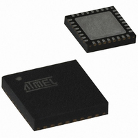
ATTINY461-20MU Atmel, ATTINY461-20MU Datasheet - Page 32

ATTINY461-20MU
Manufacturer Part Number
ATTINY461-20MU
Description
IC AVR MCU 4K 20MHZ 32-QFN
Manufacturer
Atmel
Series
AVR® ATtinyr
Specifications of ATTINY461-20MU
Core Processor
AVR
Core Size
8-Bit
Speed
20MHz
Connectivity
USI
Peripherals
Brown-out Detect/Reset, POR, PWM, WDT
Number Of I /o
16
Program Memory Size
4KB (2K x 16)
Program Memory Type
FLASH
Eeprom Size
256 x 8
Ram Size
256 x 8
Voltage - Supply (vcc/vdd)
2.7 V ~ 5.5 V
Data Converters
A/D 11x10b
Oscillator Type
Internal
Operating Temperature
-40°C ~ 85°C
Package / Case
32-VQFN Exposed Pad, 32-HVQFN, 32-SQFN, 32-DHVQFN
Processor Series
ATTINY4x
Core
AVR8
Data Bus Width
8 bit
Data Ram Size
256 B
Interface Type
2-Wire, SPI, USI
Maximum Clock Frequency
20 MHz
Number Of Programmable I/os
16
Number Of Timers
2
Maximum Operating Temperature
+ 85 C
Mounting Style
SMD/SMT
3rd Party Development Tools
EWAVR, EWAVR-BL
Development Tools By Supplier
ATAVRDRAGON, ATSTK500, ATSTK600, ATAVRISP2, ATAVRONEKIT
Minimum Operating Temperature
- 40 C
On-chip Adc
10 bit, 11 Channel
For Use With
ATSTK600-DIP40 - STK600 SOCKET/ADAPTER 40-PDIPATAVRBC100 - REF DESIGN KIT BATTERY CHARGER770-1007 - ISP 4PORT ATMEL AVR MCU SPI/JTAG
Lead Free Status / RoHS Status
Lead free / RoHS Compliant
Available stocks
Company
Part Number
Manufacturer
Quantity
Price
Company:
Part Number:
ATTINY461-20MU
Manufacturer:
KODENSHI
Quantity:
991
Company:
Part Number:
ATTINY461-20MUR
Manufacturer:
ATMEL
Quantity:
5 560
6.4
6.5
6.5.1
6.5.2
32
Clock Output Buffer
Register Description
ATtiny261/461/861
OSCCAL – Oscillator Calibration Register
CLKPR – Clock Prescale Register
From the time the CLKPS values are written, it takes between T1 + T2 and T1 + 2*T2 before the
new clock frequency is active. In this interval, two active clock edges are produced. Here, T1 is
the previous clock period, and T2 is the period corresponding to the new prescaler setting.
The device can output the system clock on the CLKO pin (when not used as XTAL2 pin). To
enable the output, the CKOUT Fuse has to be programmed. This mode is suitable when the chip
clock is used to drive other circuits on the system. Note that the clock will not be output during
reset and the normal operation of I/O pin will be overridden when the fuse is programmed. Inter-
nal RC Oscillator, WDT Oscillator, PLL, and external clock (CLKI) can be selected when the
clock is output on CLKO. Crystal oscillators (XTAL1, XTAL2) can not be used for clock output on
CLKO. If the System Clock Prescaler is used, it is the divided system clock that is output.
• Bits 7:0 – CAL7:0: Oscillator Calibration Value
The Oscillator Calibration Register is used to trim the Calibrated Internal RC Oscillator to
remove process variations from the oscillator frequency. A pre-programmed calibration value is
automatically written to this register during chip reset, giving the Factory calibrated frequency as
specified in
the oscillator frequency. The oscillator can be calibrated to frequencies as specified in
2 on page
Note that this oscillator is used to time EEPROM and Flash write accesses, and these write
times will be affected accordingly. If the EEPROM or Flash are written, do not calibrate to more
than 8.8 MHz. Otherwise, the EEPROM or Flash write may fail.
The CAL7 bit determines the range of operation for the oscillator. Setting this bit to 0 gives the
lowest frequency range, setting this bit to 1 gives the highest frequency range. The two fre-
quency ranges are overlapping, in other words a setting of OSCCAL = 0x7F gives a higher
frequency than OSCCAL = 0x80.
The CAL6:0 bits are used to tune the frequency within the selected range. A setting of 0x00
gives the lowest frequency in that range, and a setting of 0x7F gives the highest frequency in the
range.
• Bit 7 – CLKPCE: Clock Prescaler Change Enable
The CLKPCE bit must be written to logic one to enable change of the CLKPS bits. The CLKPCE
bit is only updated when the other bits in CLKPR are simultaniosly written to zero. CLKPCE is
Bit
0x31 (0x51)
Read/Write
Initial Value
Bit
0x28 (0x48)
Read/Write
Initial Value
189. Calibration outside that range is not guaranteed.
Table 19-2 on page
7
CAL7
R/W
7
CLKPCE
R/W
0
6
CAL6
R/W
6
–
R
0
5
CAL5
R/W
189. The application software can write this register to change
5
–
R
0
Device Specific Calibration Value
4
CAL4
R/W
4
–
R
0
3
CAL3
R/W
3
CLKPS3
R/W
See Bit Description
2
CAL2
R/W
2
CLKPS2
R/W
1
CAL1
R/W
1
CLKPS1
R/W
0
CAL0
R/W
0
CLKPS0
R/W
2588E–AVR–08/10
Table 19-
OSCCAL
CLKPR


