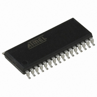
AT90PWM3B-16SU Atmel, AT90PWM3B-16SU Datasheet - Page 198

AT90PWM3B-16SU
Manufacturer Part Number
AT90PWM3B-16SU
Description
IC MCU AVR RISC 8K FLASH 32-SOIC
Manufacturer
Atmel
Series
AVR® 90PWM Lightingr
Specifications of AT90PWM3B-16SU
Core Processor
AVR
Core Size
8-Bit
Speed
16MHz
Connectivity
SPI, UART/USART
Peripherals
Brown-out Detect/Reset, POR, PWM, WDT
Number Of I /o
27
Program Memory Size
8KB (8K x 8)
Program Memory Type
FLASH
Eeprom Size
512 x 8
Ram Size
512 x 8
Voltage - Supply (vcc/vdd)
2.7 V ~ 5.5 V
Data Converters
A/D 11x10b; D/A 1x10b
Oscillator Type
Internal
Operating Temperature
-40°C ~ 105°C
Package / Case
32-SOIC (7.5mm Width)
Processor Series
AT90PWMx
Core
AVR8
Data Bus Width
8 bit
Data Ram Size
512 B
Interface Type
SPI/USART
Maximum Clock Frequency
16 MHz
Number Of Programmable I/os
27
Number Of Timers
2
Operating Supply Voltage
2.7 V to 5.5 V
Maximum Operating Temperature
+ 105 C
Mounting Style
SMD/SMT
3rd Party Development Tools
EWAVR, EWAVR-BL
Development Tools By Supplier
ATAVRDRAGON, ATSTK500, ATSTK600, ATAVRISP2, ATAVRONEKIT, ATAVRFBKIT, ATAVRISP2
Minimum Operating Temperature
- 40 C
On-chip Adc
11-ch x 10-bit
On-chip Dac
1-chx10-bit
Controller Family/series
AVR PWM
Eeprom Memory Size
512Byte
Ram Memory Size
512Byte
Cpu Speed
16MHz
Rohs Compliant
Yes
For Use With
ATSTK600-SOIC - STK600 SOCKET/ADAPTER FOR SOIC770-1007 - ISP 4PORT ATMEL AVR MCU SPI/JTAGATAVRMC200 - KIT EVAL FOR AT90PWM3 ASYNCATAVRFBKIT - KIT DEMO BALLAST FOR AT90PWM2ATAVRISP2 - PROGRAMMER AVR IN SYSTEMATSTK520 - ADAPTER KIT FOR 90PWM
Lead Free Status / RoHS Status
Lead free / RoHS Compliant
Available stocks
Company
Part Number
Manufacturer
Quantity
Price
Company:
Part Number:
AT90PWM3B-16SU
Manufacturer:
Atmel
Quantity:
4 000
Part Number:
AT90PWM3B-16SU
Manufacturer:
MICROCHIP/微芯
Quantity:
20 000
- Current page: 198 of 361
- Download datasheet (7Mb)
18.8.2
198
AT90PWM2/3/2B/3B
Asynchronous Data Recovery
figure), to decide if a valid start bit is received. If two or more of these three samples have logical
high levels (the majority wins), the start bit is rejected as a noise spike and the Receiver starts
looking for the next high to low-transition. If however, a valid start bit is detected, the clock recov-
ery logic is synchronized and the data recovery can begin. The synchronization process is
repeated for each start bit.
When the receiver clock is synchronized to the start bit, the data recovery can begin. The data
recovery unit uses a state machine that has 16 states for each bit in Normal mode and eight
states for each bit in Double Speed mode.
the parity bit. Each of the samples is given a number that is equal to the state of the recovery
unit.
Figure 18-7. Sampling of Data and Parity Bit
The decision of the logic level of the received bit is taken by doing a majority voting of the logic
value to the three samples in the center of the received bit. The center samples are emphasized
on the figure by having the sample number inside boxes. The majority voting process is done as
follows: If two or all three samples have high levels, the received bit is registered to be a logic 1.
If two or all three samples have low levels, the received bit is registered to be a logic 0. This
majority voting process acts as a low pass filter for the incoming signal on the RxD pin. The
recovery process is then repeated until a complete frame is received. Including the first stop bit.
Note that the Receiver only uses the first stop bit of a frame.
Figure 18-8
of the next frame.
Figure 18-8. Stop Bit Sampling and Next Start Bit Sampling
The same majority voting is done to the stop bit as done for the other bits in the frame. If the stop
bit is registered to have a logic 0 value, the Frame Error (FE) flag will be set.
A new high to low transition indicating the start bit of a new frame can come right after the last of
the bits used for majority voting. For Normal Speed mode, the first low level sample can be at
point marked (A) in
(B). (C) marks a stop bit of full length. The early start bit detection influences the operational
range of the Receiver.
(U2Xn = 0)
(U2Xn = 1)
(U2Xn = 0)
(U2Xn = 1)
Sample
Sample
Sample
Sample
RxDn
RxDn
shows the sampling of the stop bit and the earliest possible beginning of the start bit
Figure
1
1
1
1
18-8. For Double Speed mode the first low level must be delayed to
2
2
3
2
3
2
4
4
5
3
5
3
Figure 18-7
6
6
7
4
7
4
STOP 1
8
8
BIT x
shows the sampling of the data bits and
9
5
9
5
10
10
0/1
(A)
11
6
6
0/1
12
0/1
0/1
(B)
13
7
14
15
8
16
4317J–AVR–08/10
(C)
1
1
Related parts for AT90PWM3B-16SU
Image
Part Number
Description
Manufacturer
Datasheet
Request
R

Part Number:
Description:
Manufacturer:
Atmel Corporation
Datasheet:

Part Number:
Description:
IC MCU AVR RISC 8K FLASH 32-QFN
Manufacturer:
Atmel
Datasheet:

Part Number:
Description:
MCU AVR 8K FLASH 16MHA 32SOIC
Manufacturer:
Atmel
Datasheet:

Part Number:
Description:
IC AVR MCU FLASH 8K 32QFN
Manufacturer:
Atmel
Datasheet:

Part Number:
Description:
IC AVR MCU FLASH 8K 32SOIC
Manufacturer:
Atmel
Datasheet:

Part Number:
Description:
MCU AVR 8K FLASH 16MHZ 32-QFN
Manufacturer:
Atmel
Datasheet:

Part Number:
Description:
DEV KIT FOR AVR/AVR32
Manufacturer:
Atmel
Datasheet:

Part Number:
Description:
INTERVAL AND WIPE/WASH WIPER CONTROL IC WITH DELAY
Manufacturer:
ATMEL Corporation
Datasheet:

Part Number:
Description:
Low-Voltage Voice-Switched IC for Hands-Free Operation
Manufacturer:
ATMEL Corporation
Datasheet:

Part Number:
Description:
MONOLITHIC INTEGRATED FEATUREPHONE CIRCUIT
Manufacturer:
ATMEL Corporation
Datasheet:

Part Number:
Description:
AM-FM Receiver IC U4255BM-M
Manufacturer:
ATMEL Corporation
Datasheet:

Part Number:
Description:
Monolithic Integrated Feature Phone Circuit
Manufacturer:
ATMEL Corporation
Datasheet:

Part Number:
Description:
Multistandard Video-IF and Quasi Parallel Sound Processing
Manufacturer:
ATMEL Corporation
Datasheet:


