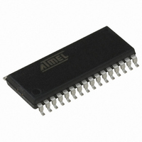
AT90PWM3B-16SU Atmel, AT90PWM3B-16SU Datasheet - Page 285

AT90PWM3B-16SU
Manufacturer Part Number
AT90PWM3B-16SU
Description
IC MCU AVR RISC 8K FLASH 32-SOIC
Manufacturer
Atmel
Series
AVR® 90PWM Lightingr
Specifications of AT90PWM3B-16SU
Core Processor
AVR
Core Size
8-Bit
Speed
16MHz
Connectivity
SPI, UART/USART
Peripherals
Brown-out Detect/Reset, POR, PWM, WDT
Number Of I /o
27
Program Memory Size
8KB (8K x 8)
Program Memory Type
FLASH
Eeprom Size
512 x 8
Ram Size
512 x 8
Voltage - Supply (vcc/vdd)
2.7 V ~ 5.5 V
Data Converters
A/D 11x10b; D/A 1x10b
Oscillator Type
Internal
Operating Temperature
-40°C ~ 105°C
Package / Case
32-SOIC (7.5mm Width)
Processor Series
AT90PWMx
Core
AVR8
Data Bus Width
8 bit
Data Ram Size
512 B
Interface Type
SPI/USART
Maximum Clock Frequency
16 MHz
Number Of Programmable I/os
27
Number Of Timers
2
Operating Supply Voltage
2.7 V to 5.5 V
Maximum Operating Temperature
+ 105 C
Mounting Style
SMD/SMT
3rd Party Development Tools
EWAVR, EWAVR-BL
Development Tools By Supplier
ATAVRDRAGON, ATSTK500, ATSTK600, ATAVRISP2, ATAVRONEKIT, ATAVRFBKIT, ATAVRISP2
Minimum Operating Temperature
- 40 C
On-chip Adc
11-ch x 10-bit
On-chip Dac
1-chx10-bit
Controller Family/series
AVR PWM
Eeprom Memory Size
512Byte
Ram Memory Size
512Byte
Cpu Speed
16MHz
Rohs Compliant
Yes
For Use With
ATSTK600-SOIC - STK600 SOCKET/ADAPTER FOR SOIC770-1007 - ISP 4PORT ATMEL AVR MCU SPI/JTAGATAVRMC200 - KIT EVAL FOR AT90PWM3 ASYNCATAVRFBKIT - KIT DEMO BALLAST FOR AT90PWM2ATAVRISP2 - PROGRAMMER AVR IN SYSTEMATSTK520 - ADAPTER KIT FOR 90PWM
Lead Free Status / RoHS Status
Lead free / RoHS Compliant
Available stocks
Company
Part Number
Manufacturer
Quantity
Price
Company:
Part Number:
AT90PWM3B-16SU
Manufacturer:
Atmel
Quantity:
4 000
Part Number:
AT90PWM3B-16SU
Manufacturer:
MICROCHIP/微芯
Quantity:
20 000
- Current page: 285 of 361
- Download datasheet (7Mb)
25.8
25.8.1
25.8.2
25.8.3
4317J–AVR–08/10
Parallel Programming
Enter Programming Mode
Considerations for Efficient Programming
Chip Erase
The following algorithm puts the device in Parallel (High-voltage) > Programming mode:
1. Set Prog_enable pins listed in Table 25-8. to “0000”, RESET pin to “0” and Vcc to 0V.
2. Apply 4.5 - 5.5V between VCC and GND. Ensure that Vcc reaches at least 1.8V within
3. Wait 20 - 60µs, and apply 11.5 - 12.5V to RESET.
4. Keep the Prog_enable pins unchanged for at least 10µs after the High-voltage has been
5. Wait at least 300µs before giving any parallel programming commands.
6. Exit Programming mode by power the device down or by bringing RESET pin to 0V.
If the rise time of the Vcc is unable to fulfill the requirements listed above, the following alterna-
tive algorithm can be used.
1. Set Prog_enable pins listed in Table 25-8. to “0000”, RESET pin to “0” and Vcc to 0V.
2. Apply 4.5 - 5.5V between VCC and GND.
3. Monitor Vcc, and as soon as Vcc reaches 0.9 - 1.1V, apply 11.5 - 12.5V to RESET.
4. Keep the Prog_enable pins unchanged for at least 10µs after the High-voltage has been
5. Wait until Vcc actually reaches 4.5 -5.5V before giving any parallel programming
6. Exit Programming mode by power the device down or by bringing RESET pin to 0V.
The loaded command and address are retained in the device during programming. For efficient
programming, the following should be considered.
•
•
•
The Chip Erase will erase the Flash and EEPROM
not reset until the program memory has been completely erased. The Fuse bits are not
changed. A Chip Erase must be performed before the Flash and/or EEPROM are
reprogrammed.
Note:
Load Command “Chip Erase”
1. Set XA1, XA0 to “10”. This enables command loading.
2. Set BS1 to “0”.
3. Set DATA to “1000 0000”. This is the command for Chip Erase.
4. Give XTAL1 a positive pulse. This loads the command.
5. Give WR a negative pulse. This starts the Chip Erase. RDY/BSY goes low.
the next 20µs.
applied to ensure the Prog_enable Signature has been latched.
applied to ensure the Prog_enable Signature has been latched.
commands.
The command needs only be loaded once when writing or reading multiple memory
locations.
Skip writing the data value 0xFF, that is the contents of the entire EEPROM (unless the
EESAVE Fuse is programmed) and Flash after a Chip Erase.
Address high byte needs only be loaded before programming or reading a new 256 word
window in Flash or 256 byte EEPROM. This consideration also applies to Signature bytes
reading.
1. The EEPRPOM memory is preserved during Chip Erase if the EESAVE Fuse is programmed.
(1)
memories plus Lock bits. The Lock bits are
AT90PWM2/3/2B/3B
285
Related parts for AT90PWM3B-16SU
Image
Part Number
Description
Manufacturer
Datasheet
Request
R

Part Number:
Description:
Manufacturer:
Atmel Corporation
Datasheet:

Part Number:
Description:
IC MCU AVR RISC 8K FLASH 32-QFN
Manufacturer:
Atmel
Datasheet:

Part Number:
Description:
MCU AVR 8K FLASH 16MHA 32SOIC
Manufacturer:
Atmel
Datasheet:

Part Number:
Description:
IC AVR MCU FLASH 8K 32QFN
Manufacturer:
Atmel
Datasheet:

Part Number:
Description:
IC AVR MCU FLASH 8K 32SOIC
Manufacturer:
Atmel
Datasheet:

Part Number:
Description:
MCU AVR 8K FLASH 16MHZ 32-QFN
Manufacturer:
Atmel
Datasheet:

Part Number:
Description:
DEV KIT FOR AVR/AVR32
Manufacturer:
Atmel
Datasheet:

Part Number:
Description:
INTERVAL AND WIPE/WASH WIPER CONTROL IC WITH DELAY
Manufacturer:
ATMEL Corporation
Datasheet:

Part Number:
Description:
Low-Voltage Voice-Switched IC for Hands-Free Operation
Manufacturer:
ATMEL Corporation
Datasheet:

Part Number:
Description:
MONOLITHIC INTEGRATED FEATUREPHONE CIRCUIT
Manufacturer:
ATMEL Corporation
Datasheet:

Part Number:
Description:
AM-FM Receiver IC U4255BM-M
Manufacturer:
ATMEL Corporation
Datasheet:

Part Number:
Description:
Monolithic Integrated Feature Phone Circuit
Manufacturer:
ATMEL Corporation
Datasheet:

Part Number:
Description:
Multistandard Video-IF and Quasi Parallel Sound Processing
Manufacturer:
ATMEL Corporation
Datasheet:


