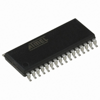
AT90PWM3B-16SU Atmel, AT90PWM3B-16SU Datasheet - Page 240

AT90PWM3B-16SU
Manufacturer Part Number
AT90PWM3B-16SU
Description
IC MCU AVR RISC 8K FLASH 32-SOIC
Manufacturer
Atmel
Series
AVR® 90PWM Lightingr
Specifications of AT90PWM3B-16SU
Core Processor
AVR
Core Size
8-Bit
Speed
16MHz
Connectivity
SPI, UART/USART
Peripherals
Brown-out Detect/Reset, POR, PWM, WDT
Number Of I /o
27
Program Memory Size
8KB (8K x 8)
Program Memory Type
FLASH
Eeprom Size
512 x 8
Ram Size
512 x 8
Voltage - Supply (vcc/vdd)
2.7 V ~ 5.5 V
Data Converters
A/D 11x10b; D/A 1x10b
Oscillator Type
Internal
Operating Temperature
-40°C ~ 105°C
Package / Case
32-SOIC (7.5mm Width)
Processor Series
AT90PWMx
Core
AVR8
Data Bus Width
8 bit
Data Ram Size
512 B
Interface Type
SPI/USART
Maximum Clock Frequency
16 MHz
Number Of Programmable I/os
27
Number Of Timers
2
Operating Supply Voltage
2.7 V to 5.5 V
Maximum Operating Temperature
+ 105 C
Mounting Style
SMD/SMT
3rd Party Development Tools
EWAVR, EWAVR-BL
Development Tools By Supplier
ATAVRDRAGON, ATSTK500, ATSTK600, ATAVRISP2, ATAVRONEKIT, ATAVRFBKIT, ATAVRISP2
Minimum Operating Temperature
- 40 C
On-chip Adc
11-ch x 10-bit
On-chip Dac
1-chx10-bit
Controller Family/series
AVR PWM
Eeprom Memory Size
512Byte
Ram Memory Size
512Byte
Cpu Speed
16MHz
Rohs Compliant
Yes
For Use With
ATSTK600-SOIC - STK600 SOCKET/ADAPTER FOR SOIC770-1007 - ISP 4PORT ATMEL AVR MCU SPI/JTAGATAVRMC200 - KIT EVAL FOR AT90PWM3 ASYNCATAVRFBKIT - KIT DEMO BALLAST FOR AT90PWM2ATAVRISP2 - PROGRAMMER AVR IN SYSTEMATSTK520 - ADAPTER KIT FOR 90PWM
Lead Free Status / RoHS Status
Lead free / RoHS Compliant
Available stocks
Company
Part Number
Manufacturer
Quantity
Price
Company:
Part Number:
AT90PWM3B-16SU
Manufacturer:
Atmel
Quantity:
4 000
Part Number:
AT90PWM3B-16SU
Manufacturer:
MICROCHIP/微芯
Quantity:
20 000
- Current page: 240 of 361
- Download datasheet (7Mb)
21.6
21.6.1
240
ADC Noise Canceler
AT90PWM2/3/2B/3B
Analog Input Circuitry
If differential channels are used, the selected reference should not be closer to AV
cated in
The ADC features a noise canceler that enables conversion during sleep mode to reduce noise
induced from the CPU core and other I/O peripherals. The noise canceler can be used with ADC
Noise Reduction and Idle mode. To make use of this feature, the following procedure should be
used:
Note that the ADC will not be automatically turned off when entering other sleep modes than Idle
mode and ADC Noise Reduction mode. The user is advised to write zero to ADEN before enter-
ing such sleep modes to avoid excessive power consumption.
If the ADC is enabled in such sleep modes and the user wants to perform differential conver-
sions, the user is advised to switch the ADC off and on after waking up from sleep to prompt an
extended conversion to get a valid result.
The analog input circuitry for single ended channels is illustrated in Figure 21-8. An analog
source applied to ADCn is subjected to the pin capacitance and input leakage of that pin, regard-
less of whether that channel is selected as input for the ADC. When the channel is selected, the
source must drive the S/H capacitor through the series resistance (combined resistance in the
input path).
The ADC is optimized for analog signals with an output impedance of approximately 10 kΩ or
less. If such a source is used, the sampling time will be negligible. If a source with higher imped-
ance is used, the sampling time will depend on how long time the source needs to charge the
S/H capacitor, with can vary widely. The user is recommended to only use low impedant sources
with slowly varying signals, since this minimizes the required charge transfer to the S/H
capacitor.
If differential gain channels are used, the input circuitry looks somewhat different, although
source impedances of a few hundred kΩ or less is recommended.
Signal components higher than the Nyquist frequency (f
kind of channels, to avoid distortion from unpredictable signal convolution. The user is advised
to remove high frequency components with a low-pass filter before applying the signals as
inputs to the ADC.
a. Make sure that the ADATE bit is reset.
b. Make sure that the ADC is enabled and is not busy converting. Single Conversion
c. Enter ADC Noise Reduction mode (or Idle mode). The ADC will start a conversion
d. If no other interrupts occur before the ADC conversion completes, the ADC inter-
Table 26-5 on page
mode must be selected and the ADC conversion complete interrupt must be
enabled.
once the CPU has been halted.
rupt will wake up the CPU and execute the ADC Conversion Complete interrupt
routine. If another interrupt wakes up the CPU before the ADC conversion is com-
plete, that interrupt will be executed, and an ADC Conversion Complete interrupt
request will be generated when the ADC conversion completes. The CPU will
remain in active mode until a new sleep command is executed.
305.
ADC
/2) should not be present for either
4317J–AVR–08/10
CC
than indi-
Related parts for AT90PWM3B-16SU
Image
Part Number
Description
Manufacturer
Datasheet
Request
R

Part Number:
Description:
Manufacturer:
Atmel Corporation
Datasheet:

Part Number:
Description:
IC MCU AVR RISC 8K FLASH 32-QFN
Manufacturer:
Atmel
Datasheet:

Part Number:
Description:
MCU AVR 8K FLASH 16MHA 32SOIC
Manufacturer:
Atmel
Datasheet:

Part Number:
Description:
IC AVR MCU FLASH 8K 32QFN
Manufacturer:
Atmel
Datasheet:

Part Number:
Description:
IC AVR MCU FLASH 8K 32SOIC
Manufacturer:
Atmel
Datasheet:

Part Number:
Description:
MCU AVR 8K FLASH 16MHZ 32-QFN
Manufacturer:
Atmel
Datasheet:

Part Number:
Description:
DEV KIT FOR AVR/AVR32
Manufacturer:
Atmel
Datasheet:

Part Number:
Description:
INTERVAL AND WIPE/WASH WIPER CONTROL IC WITH DELAY
Manufacturer:
ATMEL Corporation
Datasheet:

Part Number:
Description:
Low-Voltage Voice-Switched IC for Hands-Free Operation
Manufacturer:
ATMEL Corporation
Datasheet:

Part Number:
Description:
MONOLITHIC INTEGRATED FEATUREPHONE CIRCUIT
Manufacturer:
ATMEL Corporation
Datasheet:

Part Number:
Description:
AM-FM Receiver IC U4255BM-M
Manufacturer:
ATMEL Corporation
Datasheet:

Part Number:
Description:
Monolithic Integrated Feature Phone Circuit
Manufacturer:
ATMEL Corporation
Datasheet:

Part Number:
Description:
Multistandard Video-IF and Quasi Parallel Sound Processing
Manufacturer:
ATMEL Corporation
Datasheet:


