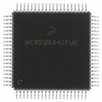
MC9S12E64CFUE Freescale Semiconductor, MC9S12E64CFUE Datasheet - Page 73

MC9S12E64CFUE
Manufacturer Part Number
MC9S12E64CFUE
Description
IC MCU 64K FLASH 25MHZ 80-QFP
Manufacturer
Freescale Semiconductor
Series
HCS12r
Specifications of MC9S12E64CFUE
Core Processor
HCS12
Core Size
16-Bit
Speed
25MHz
Connectivity
EBI/EMI, I²C, SCI, SPI
Peripherals
POR, PWM, WDT
Number Of I /o
60
Program Memory Size
64KB (64K x 8)
Program Memory Type
FLASH
Ram Size
4K x 8
Voltage - Supply (vcc/vdd)
2.35 V ~ 2.75 V
Data Converters
A/D 16x10b; D/A 2x8b
Oscillator Type
Internal
Operating Temperature
-40°C ~ 85°C
Package / Case
80-QFP
Package
80PQFP
Family Name
HCS12
Maximum Speed
25 MHz
Operating Supply Voltage
2.5|3.3|5 V
Data Bus Width
16 Bit
Number Of Programmable I/os
60
Interface Type
SCI/SPI
On-chip Adc
16-chx10-bit
On-chip Dac
2-chx8-bit
Number Of Timers
12
Processor Series
S12E
Core
HCS12
Data Ram Size
4 KB
Maximum Clock Frequency
25 MHz
Maximum Operating Temperature
+ 85 C
Mounting Style
SMD/SMT
3rd Party Development Tools
EWHCS12
Minimum Operating Temperature
- 40 C
Controller Family/series
HCS12/S12X
No. Of I/o's
58
Ram Memory Size
4KB
Cpu Speed
25MHz
No. Of Timers
4
Embedded Interface Type
I2C, SCI, SPI
Rohs Compliant
Yes
For Use With
M68EVB912E128 - BOARD EVAL FOR MC9S12E128/64
Lead Free Status / RoHS Status
Lead free / RoHS Compliant
Eeprom Size
-
Lead Free Status / Rohs Status
Lead free / RoHS Compliant
Available stocks
Company
Part Number
Manufacturer
Quantity
Price
Company:
Part Number:
MC9S12E64CFUE
Manufacturer:
Freescale Semiconductor
Quantity:
10 000
Part Number:
MC9S12E64CFUE
Manufacturer:
FREESCALE
Quantity:
20 000
Company:
Part Number:
MC9S12E64CFUER
Manufacturer:
Freescale Semiconductor
Quantity:
10 000
- Current page: 73 of 606
- Download datasheet (4Mb)
Freescale Semiconductor
VDD1, VDD2
VSS1, VSS2
Mnemonic
VDDPLL
VSSPLL
VDDR
VDDX
VSSR
VSSX
VDDA
VSSA
VRH
VRL
All VSS pins must be connected together in the application. Because fast
signal transitions place high, short-duration current demands on the power
supply, use bypass capacitors with high-frequency characteristics and place
them as close to the MCU as possible. Bypass requirements depend on
MCU pin load.
3.3/5.0 V
3.3/5.0 V
3.3/5.0 V
3.3/5.0 V
Nominal
Voltage
2.5 V
2.5 V
0 V
0 V
0 V
0 V
0 V
0V
Table 1-5. MC9S12E128 Power and Ground Connection Summary
Internal power and ground generated by internal regulator. These also allow an external
source to supply the core VDD/VSS voltages and bypass the internal voltage regulator.
External power and ground, supply to internal voltage regulator.
To disable voltage regulator attach V
External power and ground, supply to pin drivers.
Operating voltage and ground for the analog-to-digital converter, the reference for the
internal voltage regulator and the digital-to-analog converters, allows the supply voltage to
the A/D to be bypassed independently.
Reference voltage high for the ATD converter, and DAC.
Reference voltage low for the ATD converter.
Provides operating voltage and ground for the Phased-Locked Loop. This allows the
supply voltage to the PLL to be bypassed independently. Internal power and ground
generated by internal regulator.
MC9S12E128 Data Sheet, Rev. 1.07
NOTE
Chapter 1 MC9S12E128 Device Overview (MC9S12E128DGV1)
DDR
Description
to V
SSR
.
73
Related parts for MC9S12E64CFUE
Image
Part Number
Description
Manufacturer
Datasheet
Request
R
Part Number:
Description:
Manufacturer:
Freescale Semiconductor, Inc
Datasheet:
Part Number:
Description:
Manufacturer:
Freescale Semiconductor, Inc
Datasheet:
Part Number:
Description:
Manufacturer:
Freescale Semiconductor, Inc
Datasheet:
Part Number:
Description:
Manufacturer:
Freescale Semiconductor, Inc
Datasheet:
Part Number:
Description:
Manufacturer:
Freescale Semiconductor, Inc
Datasheet:
Part Number:
Description:
Manufacturer:
Freescale Semiconductor, Inc
Datasheet:
Part Number:
Description:
Manufacturer:
Freescale Semiconductor, Inc
Datasheet:
Part Number:
Description:
Manufacturer:
Freescale Semiconductor, Inc
Datasheet:
Part Number:
Description:
Manufacturer:
Freescale Semiconductor, Inc
Datasheet:
Part Number:
Description:
Manufacturer:
Freescale Semiconductor, Inc
Datasheet:
Part Number:
Description:
Manufacturer:
Freescale Semiconductor, Inc
Datasheet:
Part Number:
Description:
Manufacturer:
Freescale Semiconductor, Inc
Datasheet:
Part Number:
Description:
Manufacturer:
Freescale Semiconductor, Inc
Datasheet:
Part Number:
Description:
Manufacturer:
Freescale Semiconductor, Inc
Datasheet:
Part Number:
Description:
Manufacturer:
Freescale Semiconductor, Inc
Datasheet:


