HD64F7044F28V Renesas Electronics America, HD64F7044F28V Datasheet - Page 22
HD64F7044F28V
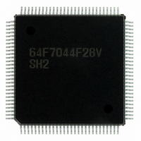
Manufacturer Part Number
HD64F7044F28V
Description
IC SUPERH MCU FLASH 112QFP
Manufacturer
Renesas Electronics America
Series
SuperH® SH7040r
Specifications of HD64F7044F28V
Core Processor
SH-2
Core Size
32-Bit
Speed
28.7MHz
Connectivity
EBI/EMI, SCI
Peripherals
DMA, POR, PWM, WDT
Number Of I /o
74
Program Memory Size
256KB (256K x 8)
Program Memory Type
FLASH
Ram Size
4K x 8
Voltage - Supply (vcc/vdd)
4.5 V ~ 5.5 V
Data Converters
A/D 8x10b
Oscillator Type
Internal
Operating Temperature
-20°C ~ 75°C
Package / Case
112-QFP
Lead Free Status / RoHS Status
Lead free / RoHS Compliant
Eeprom Size
-
Available stocks
Company
Part Number
Manufacturer
Quantity
Price
Company:

Part Number:
HD64F7044F28V
Manufacturer:
Renesas Electronics America
Quantity:
135
Company:
Part Number:
HD64F7044F28V
Manufacturer:
RENESAS
Quantity:
10
Company:
Part Number:
HD64F7044F28V
Manufacturer:
Renesas Electronics America
Quantity:
10 000
Part Number:
HD64F7044F28V
Manufacturer:
RENESAS/瑞萨
Quantity:
20 000


Section 2 Register Configuration
With DSP type instructions, eight of the 16 general registers are used in addressing the X and Y
data memory and the data memory that uses the I bus (single data).
To access X memory, R4 and R5 are used as the X address register [Ax] and R8 is used as the X
index register [Ix]. To access the Y memory, R6 and R7 are used as the Y address register [Ay]
and R9 is used as the Y index register [Iy]. To access single data using the I bus, R2, R3, R4, and
R5 are used as the single data address register and R8 as the single data index register [Is].
DSP type instructions can simultaneously access X and Y memory. There are two groups of
address pointers for specifying the X and Y data memory addresses.
Figure 2.2 shows the general registers.
Rev. 5.00 Jun 30, 2004 page 6 of 512
REJ09B0171-0500O
Notes: 1. R0 functions as an index register in the indirect indexed register addressing mode and
2. R15 functions as a hardware stack pointer (SP) during exception processing.
indirect indexed GBR addressing mode. In some instructions, R0 functions as a fixed
source register or destination register.
Figure 2.1 General Registers (SH-1 and SH-2)
31
R15, SP
R10
R11
R12
R13
R14
R0
R1
R2
R3
R4
R5
R6
R7
R8
R9
*
1
(hardware stack pointer)
*
2
0
Related parts for HD64F7044F28V
Image
Part Number
Description
Manufacturer
Datasheet
Request
R


Part Number:
Description:
KIT STARTER FOR M16C/29
Manufacturer:
Renesas Electronics America
Datasheet:

Part Number:
Description:
KIT STARTER FOR R8C/2D
Manufacturer:
Renesas Electronics America
Datasheet:

Part Number:
Description:
R0K33062P STARTER KIT
Manufacturer:
Renesas Electronics America
Datasheet:

Part Number:
Description:
KIT STARTER FOR R8C/23 E8A
Manufacturer:
Renesas Electronics America
Datasheet:

Part Number:
Description:
KIT STARTER FOR R8C/25
Manufacturer:
Renesas Electronics America
Datasheet:

Part Number:
Description:
KIT STARTER H8S2456 SHARPE DSPLY
Manufacturer:
Renesas Electronics America
Datasheet:

Part Number:
Description:
KIT STARTER FOR R8C38C
Manufacturer:
Renesas Electronics America
Datasheet:

Part Number:
Description:
KIT STARTER FOR R8C35C
Manufacturer:
Renesas Electronics America
Datasheet:

Part Number:
Description:
KIT STARTER FOR R8CL3AC+LCD APPS
Manufacturer:
Renesas Electronics America
Datasheet:
Part Number:
Description:
KIT STARTER FOR RX610
Manufacturer:
Renesas Electronics America
Datasheet:

Part Number:
Description:
KIT STARTER FOR R32C/118
Manufacturer:
Renesas Electronics America
Datasheet:

Part Number:
Description:
KIT DEV RSK-R8C/26-29
Manufacturer:
Renesas Electronics America
Datasheet:

Part Number:
Description:
KIT STARTER FOR SH7124
Manufacturer:
Renesas Electronics America
Datasheet:

Part Number:
Description:
KIT STARTER FOR H8SX/1622
Manufacturer:
Renesas Electronics America
Datasheet: