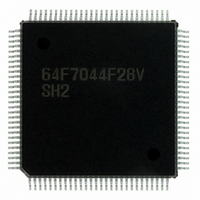
HD64F7044F28V Renesas Electronics America, HD64F7044F28V Datasheet - Page 53

HD64F7044F28V
Manufacturer Part Number
HD64F7044F28V
Description
IC SUPERH MCU FLASH 112QFP
Manufacturer
Renesas Electronics America
Series
SuperH® SH7040r
Specifications of HD64F7044F28V
Core Processor
SH-2
Core Size
32-Bit
Speed
28.7MHz
Connectivity
EBI/EMI, SCI
Peripherals
DMA, POR, PWM, WDT
Number Of I /o
74
Program Memory Size
256KB (256K x 8)
Program Memory Type
FLASH
Ram Size
4K x 8
Voltage - Supply (vcc/vdd)
4.5 V ~ 5.5 V
Data Converters
A/D 8x10b
Oscillator Type
Internal
Operating Temperature
-20°C ~ 75°C
Package / Case
112-QFP
Lead Free Status / RoHS Status
Lead free / RoHS Compliant
Eeprom Size
-
Available stocks
Company
Part Number
Manufacturer
Quantity
Price
Company:
Part Number:
HD64F7044F28V
Manufacturer:
Renesas Electronics America
Quantity:
135
Company:
Part Number:
HD64F7044F28V
Manufacturer:
RENESAS
Quantity:
10
Company:
Part Number:
HD64F7044F28V
Manufacturer:
Renesas Electronics America
Quantity:
10 000
Part Number:
HD64F7044F28V
Manufacturer:
RENESAS/瑞萨
Quantity:
20 000
- Current page: 53 of 531
- Download datasheet (3Mb)
4.5.1
The DSP command allows X and Y data memories to be accessed simultaneously using the
MOVX.W and MOVY.W instructions. DSP instructions have two pointers so they can access the
X and Y data memories simultaneously. DSP instructions have only pointer addressing; immediate
addressing is not available. Address registers are divided in two. The R4 and R5 registers become
the X memory address register (Ax) while the R6 and R7 registers become the Y memory address
register (Ay). The following three types of addressing may be used with X and Y data transfer
instructions.
Each of the address pointers has an index register. Register R8 becomes the index register (Ix) for
the X memory address register (Ax); register R9 becomes the index register (Iy) for the Y memory
address register (Ay).
X and Y data transfer instructions are processed in words. X and Y data memory is accessed in 16
bit units. Increment processing for that purpose adds two to the address register. To decrement
them, set -2 in the index register and specify addition index register addressing. For X and Y data
addressing, only bits 1 to 15 of the address pointer are valid. When performing X and Y data
addressing, make sure to write 0 to bit 0 of the address pointer and index register.
Figure 4.1 shows the X and Y data transfer addressing. With using the X or Y bus to access X
memory or Y memory, Ax (R4 or R5) and Ay (R6 or R7) upper reads [?? words] are ignored.
Also, the results of XX AY+, XX Ay + Iv are stored in the lower word of Ay, and the previous
value of the upper word is retained.
Address registers with no update: The Ax and Ay registers are address pointers. They are not
updated.
Addition index register addressing: The Ax and Ay registers are address pointers. The values
of the Ix and Iy registers are added to the Ax and Ay registers respectively after data transfer
(post-increment).
Increment address register addressing: The Ax and Ay registers are address pointers. +2 is
added to them after data transfer (post-increment).
X and Y Data Addressing
Rev. 5.00 Jun 30, 2004 page 37 of 512
Section 4 Instruction Features
REJ09B0171-0500O
Related parts for HD64F7044F28V
Image
Part Number
Description
Manufacturer
Datasheet
Request
R

Part Number:
Description:
KIT STARTER FOR M16C/29
Manufacturer:
Renesas Electronics America
Datasheet:

Part Number:
Description:
KIT STARTER FOR R8C/2D
Manufacturer:
Renesas Electronics America
Datasheet:

Part Number:
Description:
R0K33062P STARTER KIT
Manufacturer:
Renesas Electronics America
Datasheet:

Part Number:
Description:
KIT STARTER FOR R8C/23 E8A
Manufacturer:
Renesas Electronics America
Datasheet:

Part Number:
Description:
KIT STARTER FOR R8C/25
Manufacturer:
Renesas Electronics America
Datasheet:

Part Number:
Description:
KIT STARTER H8S2456 SHARPE DSPLY
Manufacturer:
Renesas Electronics America
Datasheet:

Part Number:
Description:
KIT STARTER FOR R8C38C
Manufacturer:
Renesas Electronics America
Datasheet:

Part Number:
Description:
KIT STARTER FOR R8C35C
Manufacturer:
Renesas Electronics America
Datasheet:

Part Number:
Description:
KIT STARTER FOR R8CL3AC+LCD APPS
Manufacturer:
Renesas Electronics America
Datasheet:

Part Number:
Description:
KIT STARTER FOR RX610
Manufacturer:
Renesas Electronics America
Datasheet:

Part Number:
Description:
KIT STARTER FOR R32C/118
Manufacturer:
Renesas Electronics America
Datasheet:

Part Number:
Description:
KIT DEV RSK-R8C/26-29
Manufacturer:
Renesas Electronics America
Datasheet:

Part Number:
Description:
KIT STARTER FOR SH7124
Manufacturer:
Renesas Electronics America
Datasheet:

Part Number:
Description:
KIT STARTER FOR H8SX/1622
Manufacturer:
Renesas Electronics America
Datasheet:


