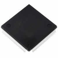
ST10F269Z2Q6 STMicroelectronics, ST10F269Z2Q6 Datasheet - Page 71

ST10F269Z2Q6
Manufacturer Part Number
ST10F269Z2Q6
Description
MCU 16BIT 256K FLASH 144PQFP
Manufacturer
STMicroelectronics
Series
ST10r
Specifications of ST10F269Z2Q6
Core Processor
ST10
Core Size
16-Bit
Speed
40MHz
Connectivity
CAN, EBI/EMI, SSC, UART/USART
Peripherals
POR, PWM, WDT
Number Of I /o
111
Program Memory Size
256KB (256K x 8)
Program Memory Type
FLASH
Ram Size
12K x 8
Voltage - Supply (vcc/vdd)
4.5 V ~ 5.5 V
Data Converters
A/D 16x10b
Oscillator Type
Internal
Operating Temperature
-40°C ~ 85°C
Package / Case
144-QFP
Controller Family/series
ST10
No. Of I/o's
111
Ram Memory Size
12KB
Cpu Speed
40MHz
No. Of Timers
5
Embedded Interface Type
CAN, SSC, USART
Rohs Compliant
Yes
Processor Series
ST10F26x
Core
ST10
Data Bus Width
16 bit
Data Ram Size
12 KB
Interface Type
CAN, SSC, USART
Maximum Clock Frequency
40 MHz
Number Of Programmable I/os
111
Number Of Timers
2 x 16 bit
Operating Supply Voltage
0.3 V to 4 V
Maximum Operating Temperature
+ 85 C
Mounting Style
SMD/SMT
Minimum Operating Temperature
- 40 C
On-chip Adc
16 bit x 10 bit
Lead Free Status / RoHS Status
Lead free / RoHS Compliant
Eeprom Size
-
Lead Free Status / Rohs Status
Details
Other names
497-4833
Available stocks
Company
Part Number
Manufacturer
Quantity
Price
Company:
Part Number:
ST10F269Z2Q6
Manufacturer:
ST
Quantity:
201
Company:
Part Number:
ST10F269Z2Q6
Manufacturer:
ST
Quantity:
745
Company:
Part Number:
ST10F269Z2Q6
Manufacturer:
STMicroelectronics
Quantity:
10 000
Part Number:
ST10F269Z2Q6
Manufacturer:
ST
Quantity:
20 000
Port 3 pins with alternate output functions are:
T6OUT, T3OUT, TxD0, BHE and CLKOUT.
When the on-chip peripheral associated with
a Port 3 pin is configured to use both the alternate
input and output function, the descriptions above
apply to the respective current operating mode.
Figure 28 : Block Diagram of Port 3 Pin with Alternate Input or Alternate Output Function
Write ODP3.y
Read ODP3.y
Write DP3.y
Open Drain
Port Output
Read DP3.y
Write DP3.y
Read P3.y
Direction
Latch
Latch
Latch
Alternate
Data
Input
MUX
Port Data
Output
1
0
Alternate
Data Output
The direction must be set accordingly. Port 3 pins
with alternate input/output functions are: MTSR,
MRST, RxD0 and SCLK.
Note: Enabling the CLKOUT function automati-
&
cally enables the P3.15 output driver. Set-
ting bit DP3.15=’1’ is not required.
Clock
Latch
Input
Output
Buffer
y = 13, 11...0
ST10F269-T3
P3.y
71/162


