M30262F6GP#U3 Renesas Electronics America, M30262F6GP#U3 Datasheet
M30262F6GP#U3
Specifications of M30262F6GP#U3
Available stocks


Related parts for M30262F6GP#U3


M30262F6GP#U3 Summary of contents
Page 1
To our customers, Old Company Name in Catalogs and Other Documents st On April 1 , 2010, NEC Electronics Corporation merged with Renesas Technology Corporation, and Renesas Electronics Corporation took over all the business of both companies. Therefore, although the ...
Page 2
All information included in this document is current as of the date this document is issued. Such information, however, is subject to change without any prior notice. Before purchasing or using any Renesas Electronics products listed herein, please confirm ...
Page 3
M16C/26 Group SINGLE-CHIP 16-BIT CMOS MICROCOMPUTER 1. Overview The M16C/26 group of single-chip microcomputers are built using the high-performance silicon gate CMOS process using a M16C/60 Series CPU core and are packaged in a 48-pin plastic molded QFP. These single-chip ...
Page 4
M16C/26 Group 1.2 Performance Outline Table 1.1 lists performance outline of M16C/26 group. Table 1.1. Performance outline of M16C/26 group Item Number of basic instructions Shortest instruction execution time Memory ROM capacity RAM I/O port P6, ...
Page 5
M16C/26 Group 1.3 Block Diagram Figure 1 block diagram of the M16C/26 group. 3 Port P6 Port P1 Internal peripheral functions Timer (16-bit) Output (timer A): 5 Input (timer B): 3 Three-phase motor control circuit Watchdog timer (15 ...
Page 6
M16C/26 Group 1.4 Product List Table 1.2 lists the M16C/26 group products, Figure 1.2 shows the type numbers, memory sizes and pack- ages, Table 1.3 lists the product code, and Figure 1.3 shows the marking. Table 1.2. Product List Type ...
Page 7
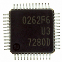
M16C/26 Group Table 1.3. Product code Product Package Program and Code Erase Endurance D3 D5 Lead-included Lead-free U7 U9 0262F8 A D3 XXXXX Figure 1.3. Marking Diagram of Flash Memory versionfor M16C/26 (Top View) Rev.1.00 2004.6.10 ...
Page 8
M16C/26 Group 1.5 Pin Configuration Figures 1.4 showd the pin configurations (top view). PIN CONFIGURATION (top view) P10 /AN / P10 /AN / P10 /AN / P10 /AN ...
Page 9
M16C/26 Group 1.6 Pin Description Table 1.4 and 1.5 describe the available pins. Table 1.4. Pin Description(1) Pin name Signal name I/O type V ,V Power supply CC SS input CNV CNV Input ____________ ...
Page 10
M16C/26 Group Table 1.7. Pin Description(2) Pin name Signal name I/O type P9 ~P9 I/O port P9 Input output P10 ~P10 I/O port P10 Input output Rev.1.00 2004.6.10 page REJ09B0176-0100Z Function This is ...
Page 11
M16C/26 Group 2. Central Processing Unit (CPU) Figure 2.1 shows the CPU registers. The CPU has 13 registers. Of these, R0, R1, R2, R3, A0, A1 and FB comprise a register bank. There are two register banks. b31 R2 R3 ...
Page 12
M16C/26 Group 2.3 Frame Base Register (FB configured with 16 bits, and is used for FB relative addressing. 2.4 Interrupt Table Register (INTB) INTB is configured with 20 bits, indicating the start address of an interrupt vector table. ...
Page 13
M16C/26 Group 3. Memory Figure 3 memory map of the M16C/26 group. The address space extends the 1M bytes from address 00000 to FFFFF . 16 16 The internal ROM is allocated in a lower address direction beginning ...
Page 14
M16C/26 Group 4. Special Function Register (SFR) Map Address 0000 16 0001 16 0002 16 0003 16 Processor mode register 0 0004 16 0005 Processor mode register 1 16 0006 System clock control register 0 16 0007 System clock control ...
Page 15
M16C/26 Group Address 0040 16 0041 16 0042 16 0043 16 INT3 interrupt control register 0044 16 0045 16 0046 16 0047 16 INT5 interrupt control register 0048 16 INT4 interrupt control register 0049 16 004A UART2 Bus collision detection ...
Page 16
M16C/26 Group Address 0080 16 0081 16 0082 16 0083 16 0084 16 0085 16 0086 01B0 16 01B1 16 01B2 16 01B3 Flash memory control register 4 16 01B4 16 01B5 Flash memory control register 1 ...
Page 17
M16C/26 Group Address 0340 16 0341 16 0342 Timer A1-1 register 16 0343 16 Timer A2-1 register 0344 16 0345 16 Timer A4-1 register 0346 16 0347 16 Three-phase PWM control register 0 0348 16 0349 Three-phase PWM control register ...
Page 18
M16C/26 Group Address 0380 Count start flag 16 Clock prescaler reset flag 0381 16 One-shot start flag 0382 16 0383 Trigger select register 16 0384 Up-down flag 16 0385 16 0386 Timer A0 register 16 0387 16 Timer A1 register ...
Page 19
M16C/26 Group Address A/D register 0 03C0 16 03C1 16 A/D register 1 03C2 16 03C3 16 A/D register 2 03C4 16 03C5 16 A/D register 3 03C6 16 03C7 16 A/D register 4 03C8 16 03C9 16 A/D register ...
Page 20
M16C/26 Group 5. Electrical Characteristics 5.1 Absolute Maximum Ratings Table 16.1. Absolute Maximum Ratings Symbol Supply voltage Analog supply voltage CC Input RESET, CNV voltage P10 0 ...
Page 21
M16C/26 Group 5.2 Recommended Operating Conditions Table 1.26.2. Recommended Operating Conditions (Note AVcc Analog supply voltage V ...
Page 22
M16C/26 Group 5.3 A/D Conversion Characteristics Table 16.3. A/D Conversion Characteristics (Note 1) Symbol Parameter – ...
Page 23
M16C/26 Group 5.4 Flash Memory Version Electrical Characteristics Table 16.4. Flash Memory Version Electrical Characteristics (Note 1) 100E/W cycle products (D3, D5, U3, U5 – ...
Page 24
M16C/26 Group 5.5 Low Voltage Detection Circuit Electrical Charactristics Table 16.7. Low Voltage Detection Circuit Electrical Characteristics (Note 1, Note ...
Page 25
M16C/26 Group 5.6 Electrical Charactristics (V Table 16.9. Electrical Characteristics (Note ...
Page 26
M16C/26 Group Table 16.10. Electrical Characteristics (2) (Note ...
Page 27
M16C/26 Group 5.7 Timing Requirements ( 5V 0V, at Topr = – Table 16.11. External Clock Input (X Symbol t External clock input cycle time External clock input ...
Page 28
M16C/26 Group Timing Requirements ( 0V, at Topr = – Table 16.12. Timer A Input (Counter Input in Event Counter Mode) Symbol t TAi input cycle time c(TA TAi ...
Page 29
M16C/26 Group Timing Requirements ( 0V, at Topr = – Table 16.18. Timer B Input (Counter Input in Event Counter Mode) Symbol t TBi input cycle time (counted on one edge) ...
Page 30
M16C/26 Group TAi input IN TAi input OUT TAi input OUT (Up/down input) During event counter mode TAi input IN (When count on falling edge is selected) TAi input IN (When count on rising edge is selected) Two-phase pulse input ...
Page 31
M16C/26 Group CLKi TxDi RxDi INTi input Figure 16.2. Timing Diagram (2) Rev.1.00 2004.6.10 page REJ09B0176-0100Z t c(CK) t w(CKH) t w(CKL su(D–C) d(C–Q) t w(INL) t w(INH) 5. Timing (V =5V ...
Page 32
M16C/26 Group 5.8 Electrical Charactristics (V Table 16.24. Electrical Characteristics (Note ...
Page 33
M16C/26 Group Table 16.25. Electrical Characteristics (2) (Note ...
Page 34
M16C/26 Group 5.9 Timing Requirements (V Timing Requirements ( 0V, at Topr = – Table 16.26. External Clock Input (X Symbol t External clock input cycle time External ...
Page 35
M16C/26 Group Timing Requirements ( 0V, at Topr = – Table 16.27. Timer A Input (Counter Input in Event Counter Mode) Symbol t TAi input cycle time c(TA TAi ...
Page 36
M16C/26 Group Timing Requirements ( 0V, at Topr = – Table 16.33. Timer B Input (Counter Input in Event Counter Mode) Symbol t TBi input cycle time (counted on one edge) ...
Page 37
M16C/26 Group TAi input IN TAi input OUT TAi input OUT (Up/down input) During event counter mode TAi input IN (When count on falling edge is selected) TAi input IN (When count on rising edge is selected) Two-phase pulse input ...
Page 38
M16C/26 Group CLKi TxDi RxDi INTi input Figure 16.4. Timing Diagram (2) Rev.1.00 2004.6.10 page REJ09B0176-0100Z t c(CK) t w(CKH) t w(CKL su(D–C) d(C–Q) t w(INL) t w(INH) 5. Timing (V =3V ...
Page 39
M16C/26 Group 6. Package 48P6Q-A Recommended EIAJ Package Code JEDEC Code LQFP48-P-77-0.50 – Rev.1.00 2004.6.10 page REJ09B0176-0100Z Weight(g) Lead Material ...
Page 40
REVISION HISTORY Rev. Date Page 1.00 Jun/10 First edition M16C/26 Hardware Manual Description Summary C-1 ...
Page 41
M16C/29 Group Keep safety first in your circuit designs! 1. Renesas Technology Corporation puts the maximum effort into making semiconductor products better and more reliable, but there is always the possibility that trouble may occur with them. Trouble with semiconductors ...