M30262F6GP#U3 Renesas Electronics America, M30262F6GP#U3 Datasheet - Page 9
M30262F6GP#U3
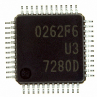
Manufacturer Part Number
M30262F6GP#U3
Description
IC M16C/TINY MCU FLASH 48LQFP
Manufacturer
Renesas Electronics America
Series
M16C™ M16C/Tiny/26r
Datasheets
1.M30622SAFPU5.pdf
(308 pages)
2.M30262F4GPU3.pdf
(41 pages)
3.M30262F4GPU3.pdf
(241 pages)
Specifications of M30262F6GP#U3
Core Processor
M16C/60
Core Size
16-Bit
Speed
20MHz
Connectivity
I²C, IEBus, SIO, UART/USART
Peripherals
DMA, WDT
Number Of I /o
38
Program Memory Size
48KB (48K x 8)
Program Memory Type
FLASH
Ram Size
2K x 8
Voltage - Supply (vcc/vdd)
2.7 V ~ 5.5 V
Data Converters
A/D 8x10b
Oscillator Type
Internal
Operating Temperature
-40°C ~ 85°C
Package / Case
48-LQFP
Lead Free Status / RoHS Status
Lead free / RoHS Compliant
Eeprom Size
-
Available stocks
Company
Part Number
Manufacturer
Quantity
Price

Part Number:
M30262F6GP#U3M30262F6GP#D3
Manufacturer:
Renesas Electronics America
Quantity:
10 000
Part Number:
M30262F6GP#U3M30262F6GP#D5
Manufacturer:
Renesas Electronics America
Quantity:
10 000
Part Number:
M30262F6GP#U3M30262F6GP#U5
Manufacturer:
Renesas Electronics America
Quantity:
10 000


M16C/26 Group
Rev.1.00
REJ09B0176-0100Z
1.6 Pin Description
Pin name Signal name
P8
P8
V
CNV
IV
____________
RESET
X
X
AV
AV
V
P1
P6
P7
Table 1.4. Pin Description(1)
CC
IN
OUT
REF
Table 1.4 and 1.5 describe the available pins.
CC
0
5
5
0
0
~P8
~P8
CC
SS
,V
~P1
~P6
~P7
SS
SS
3
7
2004.6.10
7
7
7
, I/O port P8
Power supply
input
CNV
IV
Reset input
Clock input
Clock output
Analog power
supply input
Analog power
supply input
Reference
Voltage input
I/O port P1
I/O port P6
I/O port P7
CC
SS
page 7 of 37
I/O type
Input
Input
Input
Output
Input
Input/
output
Input/
output
Input/
output
Input/
output
These pins are provided for the main clock generating circuit input/output.
Connect a ceramic resonator or crystal between the X
This pin is a reference voltage input for the A/D converter.
register that allows the user to set each pin for input or output individually.
Apply 2.7V to 5.5V to the V
Connect this pin to Vss.
Leave this pin open.
"L" on this input resets the microcomputer.
To use an externally derived clock, input it to the X
pin open.
This pin is a power supply input for the A/D converter. Connect this
pin to V
This pin is a power supply input for the A/D converter. Connect this
pin to V
This is an 3-bit CMOS I/O port. It has an input/output port direction
When used for input, a pull-up resister option can be selected for the
entire group of three pins. Additional software selectable secondary
functions are: 1) P1
pins, and; 2) P1
This is an 8-bit CMOS I/O port. It has an input/output port direction
register that allows the user to set each pin for input or output individually.
When used for input, a pull-up resister option can be selected for the
entire group of four pins. Pins in this port also function as UART0 and
UART1 I/O.
This is an 8-bit I/O port equivalent to P6. (P7
open-drain output) P7 can also function as I/O for timer A0 to A3, as
selected by software. Additional programming options are: P7
assume UART2 I/O capabilities, and P7
pins for the three-phase motor control timer.
P8
used for input, a pull-up resister option can be selected for the entire
group of four pins or three pins. Additional software-selectable secondary
functions are: 1) P8
output pins for the three-phase motor control timer; 2) P8
configured as external INT interrupt pins; 3) P8
P8
enabled. Apply a stable "H" to P8
P8
P8
case, a quartzoscillator must be connented between P8
P8
0
5
5
7
7
to "0" when the three-phase motor control is enabled, and; 4) P8
can not be used as I/O port while the three-phase motor control is
can serve as I/O pins for the sub-clock generation circuit. In this latter
(X
to P8
CIN
CC
SS
pin).
.
.
3
and P8
5
can input a trigger for the A/D converter.
5
5
0
to P8
to P1
and P8
______
7
7
are an 7-bit I/O port equivalent to P6.When
CC
can be configured as external INT interrupt
1
can act as either I/O for Timer A4, or as
pin, and 0V to the Vss pin.
Function
5
after setting the direction register for
2
to P7
0
and P7
5
5
can function as output
can be used as NMI/SD.
IN
pin and leave the X
IN
1
are N channel
and the X
6
2
(X
______
to P8
COUT
0
1. Overview
to P7
3
pin) and
_______ _____
OUT
can be
6
3
pins.
and
can
OUT
Related parts for M30262F6GP#U3
Image
Part Number
Description
Manufacturer
Datasheet
Request
R

Part Number:
Description:
KIT STARTER FOR M16C/29
Manufacturer:
Renesas Electronics America
Datasheet:

Part Number:
Description:
KIT STARTER FOR R8C/2D
Manufacturer:
Renesas Electronics America
Datasheet:

Part Number:
Description:
R0K33062P STARTER KIT
Manufacturer:
Renesas Electronics America
Datasheet:

Part Number:
Description:
KIT STARTER FOR R8C/23 E8A
Manufacturer:
Renesas Electronics America
Datasheet:

Part Number:
Description:
KIT STARTER FOR R8C/25
Manufacturer:
Renesas Electronics America
Datasheet:

Part Number:
Description:
KIT STARTER H8S2456 SHARPE DSPLY
Manufacturer:
Renesas Electronics America
Datasheet:

Part Number:
Description:
KIT STARTER FOR R8C38C
Manufacturer:
Renesas Electronics America
Datasheet:

Part Number:
Description:
KIT STARTER FOR R8C35C
Manufacturer:
Renesas Electronics America
Datasheet:

Part Number:
Description:
KIT STARTER FOR R8CL3AC+LCD APPS
Manufacturer:
Renesas Electronics America
Datasheet:
Part Number:
Description:
KIT STARTER FOR RX610
Manufacturer:
Renesas Electronics America
Datasheet:

Part Number:
Description:
KIT STARTER FOR R32C/118
Manufacturer:
Renesas Electronics America
Datasheet:

Part Number:
Description:
KIT DEV RSK-R8C/26-29
Manufacturer:
Renesas Electronics America
Datasheet:

Part Number:
Description:
KIT STARTER FOR SH7124
Manufacturer:
Renesas Electronics America
Datasheet:

Part Number:
Description:
KIT STARTER FOR H8SX/1622
Manufacturer:
Renesas Electronics America
Datasheet:

Part Number:
Description:
KIT DEV FOR SH7203
Manufacturer:
Renesas Electronics America
Datasheet: