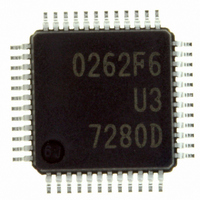
M30262F6GP#U3 Renesas Electronics America, M30262F6GP#U3 Datasheet - Page 13
M30262F6GP#U3
Manufacturer Part Number
M30262F6GP#U3
Description
IC M16C/TINY MCU FLASH 48LQFP
Manufacturer
Renesas Electronics America
Series
M16C™ M16C/Tiny/26r
Datasheets
1.M30622SAFPU5.pdf
(308 pages)
2.M30262F4GPU3.pdf
(41 pages)
3.M30262F4GPU3.pdf
(241 pages)
Specifications of M30262F6GP#U3
Core Processor
M16C/60
Core Size
16-Bit
Speed
20MHz
Connectivity
I²C, IEBus, SIO, UART/USART
Peripherals
DMA, WDT
Number Of I /o
38
Program Memory Size
48KB (48K x 8)
Program Memory Type
FLASH
Ram Size
2K x 8
Voltage - Supply (vcc/vdd)
2.7 V ~ 5.5 V
Data Converters
A/D 8x10b
Oscillator Type
Internal
Operating Temperature
-40°C ~ 85°C
Package / Case
48-LQFP
Lead Free Status / RoHS Status
Lead free / RoHS Compliant
Eeprom Size
-
Available stocks
Company
Part Number
Manufacturer
Quantity
Price

Part Number:
M30262F6GP#U3M30262F6GP#D3
Manufacturer:
Renesas Electronics America
Quantity:
10 000
Part Number:
M30262F6GP#U3M30262F6GP#D5
Manufacturer:
Renesas Electronics America
Quantity:
10 000
Part Number:
M30262F6GP#U3M30262F6GP#U5
Manufacturer:
Renesas Electronics America
Quantity:
10 000


M16C/26 Group
Rev.1.00
REJ09B0176-0100Z
3. Memory
Figure 3.1. Memory Map
Figure 3.1 is a memory map of the M16C/26 group. The address space extends the 1M bytes from address
00000
The internal ROM is allocated in a lower address direction beginning with address FFFFF
a 32-Kbyte internal ROM is allocated to the addresses from F8000
The fixed interrupt vector table is allocated to the addresses from FFFDC
the start address of each interrupt routine here.
The internal RAM is allocated in an upper address direction beginning with address 00400
a 1-Kbytes internal RAM is allocated to the addresses from 00400
the internal RAM also stores the stack used when calling subroutines and when interrupts are generated.
The SRF is allocated to the addresses from 00000
located here. Of the SFR, any area which has no functions allocated is reserved for future use and cannot
be used by users.
The special page vector table is allocated to the addresses from FFE00
by the JMPS or JSRS instruction. For details, refer to the “M16C/60 and M16C/20 Series Software Manual.”
Note 1: Shown here is a Block A (2K bytes) and Block B (2K bytes).
1K bytes
2K bytes
Size
2004.6.10
16
Internal RAM
to FFFFF
Address XXXXX
007FF
00BFF
16
16
page 11 of 37
16
16
.
24K bytes
32K bytes
48K bytes
64K bytes
Size
Internal ROM
Address YYYYY
F8000
F4000
F0000
FA000
16
16
16
16
16
XXXXX
YYYYY
0FFFF
FFFFF
0F000
00000
00400
16
16
16
16
16
16
16
16
(Program area)
Internal ROM
Reserved area
Reserved area
Internal RAM
Internal ROM
to 003FF
(Data area)
SFR
(Note 1)
16
. Peripheral function control registers are
16
16
to 007FF
to FFFFF
16
16
to FFFDB
to FFFFF
16
FFE00
FFFDC
FFFFF
16
. In addition to storing data,
.
16
16
16
16
. This vector is used
Undefined instruction
16
Watchdog timer
Special page
BRK instruction
Address match
. Therefore, store
vector table
Single step
16
16
Overflow
Reset
DBC
. For example,
. For example,
NMI
3. Memory
Related parts for M30262F6GP#U3
Image
Part Number
Description
Manufacturer
Datasheet
Request
R

Part Number:
Description:
KIT STARTER FOR M16C/29
Manufacturer:
Renesas Electronics America
Datasheet:

Part Number:
Description:
KIT STARTER FOR R8C/2D
Manufacturer:
Renesas Electronics America
Datasheet:

Part Number:
Description:
R0K33062P STARTER KIT
Manufacturer:
Renesas Electronics America
Datasheet:

Part Number:
Description:
KIT STARTER FOR R8C/23 E8A
Manufacturer:
Renesas Electronics America
Datasheet:

Part Number:
Description:
KIT STARTER FOR R8C/25
Manufacturer:
Renesas Electronics America
Datasheet:

Part Number:
Description:
KIT STARTER H8S2456 SHARPE DSPLY
Manufacturer:
Renesas Electronics America
Datasheet:

Part Number:
Description:
KIT STARTER FOR R8C38C
Manufacturer:
Renesas Electronics America
Datasheet:

Part Number:
Description:
KIT STARTER FOR R8C35C
Manufacturer:
Renesas Electronics America
Datasheet:

Part Number:
Description:
KIT STARTER FOR R8CL3AC+LCD APPS
Manufacturer:
Renesas Electronics America
Datasheet:
Part Number:
Description:
KIT STARTER FOR RX610
Manufacturer:
Renesas Electronics America
Datasheet:

Part Number:
Description:
KIT STARTER FOR R32C/118
Manufacturer:
Renesas Electronics America
Datasheet:

Part Number:
Description:
KIT DEV RSK-R8C/26-29
Manufacturer:
Renesas Electronics America
Datasheet:

Part Number:
Description:
KIT STARTER FOR SH7124
Manufacturer:
Renesas Electronics America
Datasheet:

Part Number:
Description:
KIT STARTER FOR H8SX/1622
Manufacturer:
Renesas Electronics America
Datasheet:

Part Number:
Description:
KIT DEV FOR SH7203
Manufacturer:
Renesas Electronics America
Datasheet: