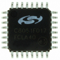
C8051F017-GQ Silicon Laboratories Inc, C8051F017-GQ Datasheet - Page 141

C8051F017-GQ
Manufacturer Part Number
C8051F017-GQ
Description
IC 8051 MCU 32K FLASH 32LQFP
Manufacturer
Silicon Laboratories Inc
Series
C8051F01xr
Specifications of C8051F017-GQ
Program Memory Type
FLASH
Program Memory Size
32KB (32K x 8)
Package / Case
32-LQFP
Core Processor
8051
Core Size
8-Bit
Speed
25MHz
Connectivity
SMBus (2-Wire/I²C), SPI, UART/USART
Peripherals
Brown-out Detect/Reset, POR, PWM, Temp Sensor, WDT
Number Of I /o
8
Ram Size
2.25K x 8
Voltage - Supply (vcc/vdd)
2.7 V ~ 3.6 V
Data Converters
A/D 4x10b; D/A 2x12b
Oscillator Type
Internal
Operating Temperature
-40°C ~ 85°C
Processor Series
C8051F0x
Core
8051
Data Bus Width
8 bit
Data Ram Size
2.25 KB
Interface Type
I2C/SMBus/SPI/UART
Maximum Clock Frequency
25 MHz
Number Of Programmable I/os
8
Number Of Timers
4
Operating Supply Voltage
2.7 V to 3.6 V
Maximum Operating Temperature
+ 85 C
Mounting Style
SMD/SMT
3rd Party Development Tools
PK51, CA51, A51, ULINK2
Development Tools By Supplier
C8051F005DK
Minimum Operating Temperature
- 40 C
On-chip Adc
4-ch x 10-bit
On-chip Dac
2-ch x 12-bit
No. Of I/o's
8
Ram Memory Size
256Byte
Cpu Speed
25MHz
No. Of Timers
4
No. Of Pwm Channels
5
Rohs Compliant
Yes
Lead Free Status / RoHS Status
Lead free / RoHS Compliant
Eeprom Size
-
Lead Free Status / Rohs Status
Lead free / RoHS Compliant
Other names
336-1196
Available stocks
Company
Part Number
Manufacturer
Quantity
Price
Company:
Part Number:
C8051F017-GQ
Manufacturer:
Silicon Labs
Quantity:
135
Company:
Part Number:
C8051F017-GQ
Manufacturer:
Silicon Laboratories Inc
Quantity:
10 000
Company:
Part Number:
C8051F017-GQR
Manufacturer:
Silicon Laboratories Inc
Quantity:
10 000
19.1.4. Mode 3: Two 8-bit Counter/Timers (Timer 0 Only)
Timer 0 and Timer 1 behave differently in Mode 3. Timer 0 is configured as two separate 8-bit counter/timers held
in TL0 and TH0. The counter/timer in TL0 is controlled using the Timer 0 control/status bits in TCON and TMOD:
TR0, C/T0, GATE0 and TF0. It can use either the system clock or an external input signal as its timebase. The
TH0 register is restricted to a timer function sourced by the system clock. TH0 is enabled using the Timer 1 run
control bit TR1. TH0 sets the Timer 1 overflow flag TF1 on overflow and thus controls the Timer 1 interrupt.
Timer 1 is inactive in Mode 3, so with Timer 0 in Mode 3, Timer 1 can be turned off and on by switching it into and
out of its Mode 3. When Timer 0 is in Mode 3, Timer 1 can be operated in Modes 0, 1 or 2, but cannot be clocked
by external signals nor set the TF1 flag and generate an interrupt. However, the Timer 1 overflow can be used for
baud rate generation. Refer to Section 18 (UART) for information on configuring Timer 1 for baud rate generation.
141
C8051F000/1/2/5/6/7
C8051F010/1/2/5/6/7
SYSCLK
/INT0
T0
GATE0
Crossbar
Crossbar
12
TR0
TR1
0
1
Figure 19.3. T0 Mode 3 Block Diagram
CKCON
M
T
2
M
T
1
M
T
0
0
1
C/T0
G
A
T
E
1
Rev. 1.7
C
T
1
/
M
T
1
1
TMOD
M
T
1
0
G
A
T
E
0
C
T
0
/
M
T
0
1
M
T
0
0
(8 bits)
(8 bits)
TH0
TL0
TR1
TR0
TF1
TF0
IE1
IT1
IE0
IT0
Interrupt
Interrupt


