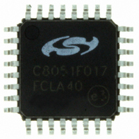
C8051F017-GQ Silicon Laboratories Inc, C8051F017-GQ Datasheet - Page 46

C8051F017-GQ
Manufacturer Part Number
C8051F017-GQ
Description
IC 8051 MCU 32K FLASH 32LQFP
Manufacturer
Silicon Laboratories Inc
Series
C8051F01xr
Specifications of C8051F017-GQ
Program Memory Type
FLASH
Program Memory Size
32KB (32K x 8)
Package / Case
32-LQFP
Core Processor
8051
Core Size
8-Bit
Speed
25MHz
Connectivity
SMBus (2-Wire/I²C), SPI, UART/USART
Peripherals
Brown-out Detect/Reset, POR, PWM, Temp Sensor, WDT
Number Of I /o
8
Ram Size
2.25K x 8
Voltage - Supply (vcc/vdd)
2.7 V ~ 3.6 V
Data Converters
A/D 4x10b; D/A 2x12b
Oscillator Type
Internal
Operating Temperature
-40°C ~ 85°C
Processor Series
C8051F0x
Core
8051
Data Bus Width
8 bit
Data Ram Size
2.25 KB
Interface Type
I2C/SMBus/SPI/UART
Maximum Clock Frequency
25 MHz
Number Of Programmable I/os
8
Number Of Timers
4
Operating Supply Voltage
2.7 V to 3.6 V
Maximum Operating Temperature
+ 85 C
Mounting Style
SMD/SMT
3rd Party Development Tools
PK51, CA51, A51, ULINK2
Development Tools By Supplier
C8051F005DK
Minimum Operating Temperature
- 40 C
On-chip Adc
4-ch x 10-bit
On-chip Dac
2-ch x 12-bit
No. Of I/o's
8
Ram Memory Size
256Byte
Cpu Speed
25MHz
No. Of Timers
4
No. Of Pwm Channels
5
Rohs Compliant
Yes
Lead Free Status / RoHS Status
Lead free / RoHS Compliant
Eeprom Size
-
Lead Free Status / Rohs Status
Lead free / RoHS Compliant
Other names
336-1196
Available stocks
Company
Part Number
Manufacturer
Quantity
Price
Company:
Part Number:
C8051F017-GQ
Manufacturer:
Silicon Labs
Quantity:
135
Company:
Part Number:
C8051F017-GQ
Manufacturer:
Silicon Laboratories Inc
Quantity:
10 000
Company:
Part Number:
C8051F017-GQR
Manufacturer:
Silicon Laboratories Inc
Quantity:
10 000
Bits7-0: ADC Data Word Bits
Bits7-0: ADC Data Word Bits
R/W
R/W
Bit7
Bit7
NOTE: Resulting 10-bit ADC Data Word appears in the ADC Data Word Registers as follows:
ADC0H[1:0]:ADC0L[7:0], if ADLJST = 0
ADC0H[7:0]:ADC0L[7:6], if ADLJST = 1
EXAMPLE: ADC Data Word Conversion Map, AIN0 Input in Single-Ended Mode
EXAMPLE: ADC Data Word Conversion Map, AIN0-AIN1 Differential Input Pair
AIN0 – AGND
(Volts)
REF x (1023/1024)
REF x ½
REF x (511/1024)
0
AIN0 – AIN1 (Volts)
REF x (511/512)
0
-REF x (1/512)
-REF
For ADLJST = 1: Upper 8-bits of the 10-bit ADC Data Word.
For ADLJST = 0: Bits7-2 are the sign extension of Bit1. Bits 1-0 are the upper 2-bits of the
10-bit ADC Data Word.
For ADLJST = 1: Bits7-6 are the lower 2-bits of the 10-bit ADC Data Word. Bits5-0 will
always read 0.
For ADLJST = 0: Bits7-0 are the lower 8-bits of the 10-bit ADC Data Word.
Figure 6.8. ADC0H: ADC Data Word MSB Register (C8051F01x)
Figure 6.9. ADC0L: ADC Data Word LSB Register (C8051F01x)
(ADC0H[7:2] will be sign extension of ADC0H.1 if a differential reading, otherwise = 000000b)
(ADC0L[5:0] = 000000b)
R/W
R/W
Bit6
Bit6
(AMX0CF=0x00, AMX0SL=0x00)
(AMX0CF=0x01, AMX0SL=0x00)
R/W
R/W
Bit5
Bit5
ADC0H:ADC0L
(ADLJST = 0)
0x03FF
0x0200
0x01FF
0x0000
ADC0H:ADC0L
(ADLJST = 0)
0x01FF
0x0000
0xFFFF
0xFE00
R/W
R/W
Bit4
Bit4
Rev. 1.7
R/W
R/W
Bit3
Bit3
ADC0H:ADC0L
(ADLJST = 1)
0xFFC0
0x8000
0x7FC0
0x0000
ADC0H:ADC0L
(ADLJST = 1)
0x7FC0
0x0000
0xFFC0
0x8000
R/W
R/W
Bit2
Bit2
C8051F000/1/2/5/6/7
C8051F010/1/2/5/6/7
R/W
R/W
Bit1
Bit1
R/W
R/W
Bit0
Bit0
SFR Address:
SFR Address:
Reset Value
Reset Value
00000000
00000000
0xBE
0xBF
46


