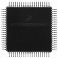
MC9S12XDT256MAA Freescale Semiconductor, MC9S12XDT256MAA Datasheet - Page 802

MC9S12XDT256MAA
Manufacturer Part Number
MC9S12XDT256MAA
Description
IC MCU 256K FLASH 80-QFP
Manufacturer
Freescale Semiconductor
Series
HCS12r
Datasheet
1.MC9S12XD64CAA.pdf
(1348 pages)
Specifications of MC9S12XDT256MAA
Core Processor
HCS12X
Core Size
16-Bit
Speed
80MHz
Connectivity
CAN, EBI/EMI, I²C, IrDA, LIN, SCI, SPI
Peripherals
LVD, POR, PWM, WDT
Number Of I /o
59
Program Memory Size
256KB (256K x 8)
Program Memory Type
FLASH
Eeprom Size
4K x 8
Ram Size
16K x 8
Voltage - Supply (vcc/vdd)
2.35 V ~ 5.5 V
Data Converters
A/D 8x10b
Oscillator Type
External
Operating Temperature
-40°C ~ 125°C
Package / Case
80-QFP
Cpu Family
HCS12
Device Core Size
16b
Frequency (max)
40MHz
Interface Type
CAN/I2C/SCI/SPI
Total Internal Ram Size
16KB
# I/os (max)
59
Number Of Timers - General Purpose
12
Operating Supply Voltage (typ)
2.5/5V
Operating Supply Voltage (max)
2.75/5.5V
Operating Supply Voltage (min)
2.35/3.15V
On-chip Adc
8-chx10-bit
Instruction Set Architecture
CISC
Operating Temp Range
-40C to 125C
Operating Temperature Classification
Automotive
Mounting
Surface Mount
Pin Count
80
Package Type
PQFP
Processor Series
S12XD
Core
HCS12
Data Bus Width
16 bit
Data Ram Size
16 KB
Maximum Clock Frequency
40 MHz
Number Of Programmable I/os
59
Number Of Timers
12
Operating Supply Voltage
0 V to 5.5 V
Maximum Operating Temperature
+ 125 C
Mounting Style
SMD/SMT
3rd Party Development Tools
EWHCS12
Development Tools By Supplier
EVB9S12XDP512E
Minimum Operating Temperature
- 40 C
Lead Free Status / RoHS Status
Lead free / RoHS Compliant
Available stocks
Company
Part Number
Manufacturer
Quantity
Price
Company:
Part Number:
MC9S12XDT256MAA
Manufacturer:
Freescale Semiconductor
Quantity:
10 000
- Current page: 802 of 1348
- Download datasheet (8Mb)
Chapter 21 External Bus Interface (S12XEBIV2)
21.5.2.1
This mode is used for emulation systems in which the target application is operating in normal single-chip
mode.
Figure 21-5
The timing diagram for this operation is shown in:
The associated timing numbers are given in:
Timing considerations:
804
•
•
•
•
•
•
Figure ‘Example 2a: Emulation Single-Chip Mode — Read Followed by Write’
Table ‘Example 2a: Emulation Single-Chip Mode Timing (EWAITE = 0)’
Signals muxed with address lines ADDRx, i.e., IVDx, IQSTATx and ACCx, have the same timing.
LSTRB has the same timing as R/W.
ECLKX2 rising edges have the same timing as ECLK edges.
The timing for accesses to PRU registers, which take 2 cycles to complete, is the same as the timing
for an external non-PRR access with 1 cycle of stretch as shown in example 2b.
shows the PRU connection with the available external bus signals in an emulator application.
Example 2a: Emulation Single-Chip Mode
Figure 21-5. Application in Emulation Single-Chip Mode
ADDR[22:20]/ACC[2:0]
ADDR[22:0]/IVD[15:0]
S12X_EBI
ADDR[19:16]/
IQSTAT[3:0]
DATA[15:0]
MC9S12XDP512 Data Sheet, Rev. 2.21
ECLKX2
LSTRB
ECLK
R/W
EMULMEM
PRU
Emulator
PRR
Ports
Freescale Semiconductor
Related parts for MC9S12XDT256MAA
Image
Part Number
Description
Manufacturer
Datasheet
Request
R

Part Number:
Description:
16-BIT MICROPROCESSOR FAMILY
Manufacturer:
FREESCALE [Freescale Semiconductor, Inc]
Datasheet:
Part Number:
Description:
Manufacturer:
Freescale Semiconductor, Inc
Datasheet:
Part Number:
Description:
Manufacturer:
Freescale Semiconductor, Inc
Datasheet:
Part Number:
Description:
Manufacturer:
Freescale Semiconductor, Inc
Datasheet:
Part Number:
Description:
Manufacturer:
Freescale Semiconductor, Inc
Datasheet:
Part Number:
Description:
Manufacturer:
Freescale Semiconductor, Inc
Datasheet:
Part Number:
Description:
Manufacturer:
Freescale Semiconductor, Inc
Datasheet:
Part Number:
Description:
Manufacturer:
Freescale Semiconductor, Inc
Datasheet:
Part Number:
Description:
Manufacturer:
Freescale Semiconductor, Inc
Datasheet:
Part Number:
Description:
Manufacturer:
Freescale Semiconductor, Inc
Datasheet:
Part Number:
Description:
Manufacturer:
Freescale Semiconductor, Inc
Datasheet:
Part Number:
Description:
Manufacturer:
Freescale Semiconductor, Inc
Datasheet:
Part Number:
Description:
Manufacturer:
Freescale Semiconductor, Inc
Datasheet:
Part Number:
Description:
Manufacturer:
Freescale Semiconductor, Inc
Datasheet:
Part Number:
Description:
Manufacturer:
Freescale Semiconductor, Inc
Datasheet:


