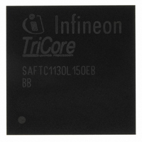
SAF-TC1130-L150EB-G BB Infineon Technologies, SAF-TC1130-L150EB-G BB Datasheet - Page 21

SAF-TC1130-L150EB-G BB
Manufacturer Part Number
SAF-TC1130-L150EB-G BB
Description
IC MCU 32BIT TRICOR 16KB LBGA208
Manufacturer
Infineon Technologies
Series
TC11xxr
Datasheet
1.SAF-TC1130-L100EB-G_BB.pdf
(114 pages)
Specifications of SAF-TC1130-L150EB-G BB
Core Processor
TriCore
Core Size
32-Bit
Speed
150MHz
Connectivity
CAN, EBI/EMI, FIFO, I²C, IrDA, SPI, UART/USART, USB
Peripherals
DMA, POR, PWM, WDT
Number Of I /o
72
Program Memory Type
ROMless
Ram Size
144K x 8
Voltage - Supply (vcc/vdd)
1.43 V ~ 1.58 V
Oscillator Type
External
Operating Temperature
-40°C ~ 85°C
Package / Case
208-LSBGA
Data Bus Width
32 bit
Program Memory Size
32 KB
Data Ram Size
144 KB
Interface Type
3xASC, 2xSSC, I2C, 2xMLI, Ethernet 10, 100 Mbits, s, USB
Maximum Clock Frequency
150 MHz
Number Of Programmable I/os
72
Number Of Timers
9
Operating Supply Voltage
1.5 V, 3.3 V
Maximum Operating Temperature
+ 85 C
Mounting Style
SMD/SMT
Minimum Operating Temperature
- 40 C
Packages
PG-LBGA-208
Max Clock Frequency
150.0 MHz
Sram (incl. Cache)
144.0 KByte
Can Nodes
4
Program Memory
0.0 KByte
Lead Free Status / RoHS Status
Lead free / RoHS Compliant
Eeprom Size
-
Program Memory Size
-
Data Converters
-
Lead Free Status / Rohs Status
Details
Other names
FT1130L150EBGBBXP
SAF-TC1130-L150EB-GBB
SAF-TC1130-L150EB-GBBINTR
SAF-TC1130-L150EB-GBBTR
SAF-TC1130-L150EB-GBBTR
SAFTC1130L150EBBBXT
SP000106119
SP000106538
SP000743584
SAF-TC1130-L150EB-GBB
SAF-TC1130-L150EB-GBBINTR
SAF-TC1130-L150EB-GBBTR
SAF-TC1130-L150EB-GBBTR
SAFTC1130L150EBBBXT
SP000106119
SP000106538
SP000743584
Table 2-1
Symbol
TRST
TCK
TDI
TDO
TMS
TRCLK
HWCFG0
HWCFG1
HWCFG2
BRKIN
MII_
TXCLK
MII_
RXCLK
MII_
MDIO
D+
Data Sheet
Pin
T11
T12
T13
T10
T9
T8
M14
L14
T6
T5
T2
R2
R1
T14
Pin Definitions and Functions (cont’d)
In
Out
I
I
I
O
I
O
I
I
I
I
I
I
I/O
I/O
PU/
PD
PDC JTAG Module Reset/Enable Input
PUC JTAG Module Clock Input
PUC JTAG Module Serial Data Input
⎯
PUC JTAG Module State Machine Control Input
⎯
PUC
PUC
PDC
PUC OCDS Break Input
PDC Ethernet Controller Transmit Clock
PDC Ethernet Controller Receive Clock
PDA
⎯
1)
Functions
A low level at this pin resets and disables the JTAG
module. A high level enables the JTAG module.
JTAG Module Serial Data Output
Trace Clock for OCDS_L2 Lines
Hardware Configuration Inputs
The Configuration Inputs define the boot options of the
TC1130 after a hardware invoked reset operation.
A low level on this pin causes a break in the chip’s
execution when the OCDS is enabled. In addition, the
level of this pin during power-on reset determines the
boot configuration.
MII_TXD[3:0] and MII_TXEN are driven off the rising
edge of the MII_TXCLK by the core and sampled by
the PHY on the rising edge of the MII_TXCLK.
MII_RXCLK is a continuous clock. Its frequency is
25 MHz for 100 Mbit/sec operation, and 2.5 MHz for
10 Mbit/sec. MII_RXD[3:0], MII_RXDV and MII_EXER
are driven by the PHY off the falling edge of
MII_RXCLK and sampled on the rising edge of
MII_RXCLK.
Ethernet Controller Management Data Input/
Output
When a read command is being executed, the data
that is clocked out of the PHY will be presented on the
input line. When the Core is clocking control or data
onto the MII_MDIO line, the signal will carry the
information.
USB D+ Data Line
15
General Device Information
V1.1, 2008-12
TC1130


