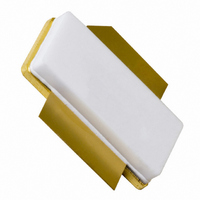
BLF6G22LS-180RN:11 NXP Semiconductors, BLF6G22LS-180RN:11 Datasheet - Page 5

BLF6G22LS-180RN:11
Manufacturer Part Number
BLF6G22LS-180RN:11
Description
BLF6G22LS-180RN/LDMOST/REEL13/
Manufacturer
NXP Semiconductors
Datasheet
1.BLF6G22LS-180RN11.pdf
(11 pages)
Specifications of BLF6G22LS-180RN:11
Transistor Type
LDMOS
Frequency
2.11GHz
Gain
16dB
Voltage - Rated
65V
Current Rating
49A
Current - Test
1.4A
Voltage - Test
30V
Power - Output
40W
Package / Case
SOT502B
Lead Free Status / RoHS Status
Lead free / RoHS Compliant
Noise Figure
-
Lead Free Status / RoHS Status
Lead free / RoHS Compliant
Other names
934062734118
NXP Semiconductors
8. Test information
BLF6G22-180RN_22LS-180RN_1
Product data sheet
Fig 4.
(dB)
G
p
17
16
15
14
0
V
carrier spacing 10 MHz.
2-carrier W-CDMA power gain and drain
efficiency as function of average load power;
typical values
DS
= 30 V; I
7.4 2-carrier W-CDMA
Dq
20
= 1400 mA; f = 2140 MHz ( 5 MHz);
G
Fig 6.
D
p
input
C1
V
GG
C7
The drawing is not to scale.
Test circuit for operation at 2200 MHz
40
P
C8
L(AV)
R2
001aai644
C6
C5
C4
(W)
Rev. 01 — 20 November 2008
R1
60
60
40
20
0
(%)
D
C3
C2
Fig 5.
ACPR
IMD3
(dBc)
30
35
40
45
50
55
0
V
carrier spacing 10 MHz.
2-carrier W-CDMA adjacent channel power
ratio and third order intermodulation distortion
as function of average load power; typical
values
DS
BLF6G22(LS)-180RN
= 30 V; I
Dq
20
= 1400 mA; f = 2140 MHz ( 5 MHz);
C12
C13
C9
ACPR
C17
IMD3
Power LDMOS transistor
C14
V
DD
40
C10
C18
C20
P
C15
L(AV)
© NXP B.V. 2008. All rights reserved.
001aai645
C19
(W)
C11
C16
60
001aai646
output
5 of 11


