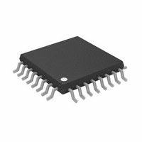
AD7265BSUZ Analog Devices Inc, AD7265BSUZ Datasheet - Page 19

AD7265BSUZ
Manufacturer Part Number
AD7265BSUZ
Description
IC,Data Acquisition System,3-CHANNEL,12-BIT,TQFP,32PIN,PLASTIC
Manufacturer
Analog Devices Inc
Datasheet
1.AD7265BCPZ-REEL.pdf
(28 pages)
Specifications of AD7265BSUZ
Design Resources
AD7265 in Differential and Single-Ended Configurations Using AD8022 (CN0048)
Number Of Bits
12
Sampling Rate (per Second)
1M
Data Interface
DSP, MICROWIRE™, QSPI™, Serial, SPI™
Number Of Converters
2
Power Dissipation (max)
21mW
Voltage Supply Source
Analog and Digital
Operating Temperature
-40°C ~ 125°C
Mounting Type
Surface Mount
Package / Case
32-TQFP, 32-VQFP
Number Of Elements
2
Resolution
12Bit
Architecture
SAR
Sample Rate
1MSPS
Input Polarity
Unipolar
Input Type
Voltage
Rated Input Volt
2.5/5V
Differential Input
Yes
Power Supply Requirement
Analog and Digital
Single Supply Voltage (typ)
3/5V
Single Supply Voltage (min)
2.7V
Single Supply Voltage (max)
5.25V
Dual Supply Voltage (typ)
Not RequiredV
Dual Supply Voltage (min)
Not RequiredV
Dual Supply Voltage (max)
Not RequiredV
Power Dissipation
21mW
Differential Linearity Error
-0.99LSB/1.5LSB
Integral Nonlinearity Error
±1.5LSB
Operating Temp Range
-40C to 125C
Operating Temperature Classification
Automotive
Mounting
Surface Mount
Pin Count
32
Package Type
TQFP
Lead Free Status / RoHS Status
Lead free / RoHS Compliant
For Use With
EVAL-AD7265CB - BOARD EVALUATION FOR AD7265
Lead Free Status / Rohs Status
Compliant
Available stocks
Company
Part Number
Manufacturer
Quantity
Price
Company:
Part Number:
AD7265BSUZ
Manufacturer:
ADI
Quantity:
200
Company:
Part Number:
AD7265BSUZ
Manufacturer:
Analog Devices Inc
Quantity:
10 000
Company:
Part Number:
AD7265BSUZ-REEL
Manufacturer:
Analog Devices Inc
Quantity:
10 000
Company:
Part Number:
AD7265BSUZ-REEL7
Manufacturer:
Analog Devices Inc
Quantity:
10 000
Part Number:
AD7265BSUZ-REEL7
Manufacturer:
ADI/亚德诺
Quantity:
20 000
MODES OF OPERATION
The mode of operation of the AD7265 is selected by controlling
the (logic) state of the
three possible modes of operation: normal mode, partial power-
down mode, and full power-down mode. After a conversion is
initiated, the point at which
power-down mode, if any, the device enters. Similarly, if already
in a power-down mode,
returns to normal operation or remains in power-down. These
modes of operation are designed to provide flexible power
management options. These options can be chosen to optimize
the power dissipation/throughput rate ratio for differing
application requirements.
NORMAL MODE
This mode is intended for applications that need the fastest
throughput rates because the user does not have to worry about
any power-up times with the AD7265 remaining fully powered
at all times. Figure 34 shows the general diagram of the
operation of the AD7265 in this mode.
The conversion is initiated on the falling edge of CS , as
described in the Serial Interface section. To ensure that the part
remains fully powered up at all times, CS must remain low until
at least 10 SCLK falling edges have elapsed after the falling edge
of CS . If CS is brought high any time after the 10
edge but before the 14
powered up, but the conversion is terminated and D
D
required to complete the conversion and access the conversion
result. The D
SCLK cycles have elapsed, but instead does so when CS is
brought high again. If CS is left low for another 2 SCLK cycles
(for example, if only a 16 SCLK burst is available), two trailing
zeros are clocked out after the data. If CS is left low for a further
14 (or 16) SCLK cycles, the result from the other ADC on board
is also accessed on the same D
(see the Serial Interface section).
D
D
SCLK
OUT
OUT
OUT
CS
A
B
B go back into three-state. Fourteen serial clock cycles are
OUT
1
line does not return to three-state after 14
LEADING ZEROS + CONVERSION RESULT
Figure 34. Normal Mode Operation
th
CS signal during a conversion. There are
SCLK falling edge, the part remains
CS can control whether the device
CS is pulled high determines which
OUT
line, as shown in Figure 42
10
th
14
SCLK falling
OUT
A and
Rev. A | Page 19 of 28
Once 32 SCLK cycles have elapsed, the D
three-state on the 32
prior to this, the D
Therefore, CS may idle low after 32 SCLK cycles until it is
brought high again sometime prior to the next conversion
(effectively idling
returns to three-state upon completion of the dual result read.
Once a data transfer is complete and D
returned to three-state, another conversion can be initiated after
the quiet time, t
(assuming the required acquisition time is allowed).
PARTIAL POWER-DOWN MODE
This mode is intended for use in applications where slower
throughput rates are required. Either the ADC is powered down
between each conversion, or a series of conversions may be
performed at a high throughput rate, and the ADC is then
powered down for a relatively long duration between these
bursts of several conversions. When the AD7265 is in partial
power-down, all analog circuitry is powered down except for
the on-chip reference and reference buffer.
To enter partial power-down mode, the conversion process
must be interrupted by bringing CS high anywhere after the
second falling edge of SCLK and before the 10
SCLK, as shown in
window of SCLKs, the part enters partial power-down, the
conversion that was initiated by the falling edge of CS is
terminated, and D
CS is brought high before the second SCLK falling edge, the
part remains in normal mode and does not power down. This
avoids accidental power-down due to glitches on the CS line.
D
D
SCLK
OUT
OUT
CS
A
B
Figure 35. Entering Partial Power-Down Mode
QUIET
1
CS low), if so desired, because the bus still
OUT
2
OUT
Figure 35. Once
, has elapsed by bringing
nd
A and D
line returns to three-state at that point.
SCLK falling edge. If
OUT
B go back into three-state. If
CS
OUT
is brought high in this
10
THREE-STATE
OUT
A and D
CS
line returns to
CS
th
is brought high
falling edge of
low again
OUT
1
4
AD7265
B have


