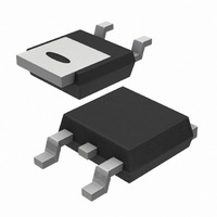
BUK9219-55A,118 NXP Semiconductors, BUK9219-55A,118 Datasheet - Page 5

BUK9219-55A,118
Manufacturer Part Number
BUK9219-55A,118
Description
MOSFET N-CH 55V 55A DPAK
Manufacturer
NXP Semiconductors
Series
TrenchMOS™r
Datasheet
1.BUK9219-55A118.pdf
(14 pages)
Specifications of BUK9219-55A,118
Package / Case
DPak, TO-252 (2 leads+tab), SC-63
Fet Type
MOSFET N-Channel, Metal Oxide
Fet Feature
Logic Level Gate
Rds On (max) @ Id, Vgs
17.6 mOhm @ 25A, 10V
Drain To Source Voltage (vdss)
55V
Current - Continuous Drain (id) @ 25° C
55A
Vgs(th) (max) @ Id
2V @ 1mA
Input Capacitance (ciss) @ Vds
2920pF @ 25V
Power - Max
114W
Mounting Type
Surface Mount
Minimum Operating Temperature
- 55 C
Configuration
Single Dual Drain
Transistor Polarity
N-Channel
Resistance Drain-source Rds (on)
0.0176 Ohm @ 10 V
Drain-source Breakdown Voltage
55 V
Gate-source Breakdown Voltage
+/- 10 V
Continuous Drain Current
55 A
Power Dissipation
114000 mW
Maximum Operating Temperature
+ 175 C
Mounting Style
SMD/SMT
Lead Free Status / RoHS Status
Lead free / RoHS Compliant
Gate Charge (qg) @ Vgs
-
Lead Free Status / Rohs Status
Lead free / RoHS Compliant
Other names
934056240118
BUK9219-55A /T3
BUK9219-55A /T3
BUK9219-55A /T3
BUK9219-55A /T3
NXP Semiconductors
5. Thermal characteristics
Table 5.
BUK9219-55A
Product data sheet
Symbol
R
R
Fig 4.
th(j-mb)
th(j-a)
Transient thermal impedance from junction to mounting base as a function of pulse duration
Thermal characteristics
Parameter
thermal resistance from junction to
mounting base
thermal resistance from junction to
ambient
Z
(K/W)
th(j-mb)
10
10
10
10
−1
−2
−3
1
10
−6
0.02
0.2
0.1
0.05
δ = 0.5
Single Shot
10
−5
All information provided in this document is subject to legal disclaimers.
10
−4
Rev. 02 — 7 June 2010
Conditions
see
minimum footprint ; FR4
board
Figure 4
10
−3
10
−2
N-channel TrenchMOS logic level FET
P
10
t
p
−1
T
t
p
BUK9219-55A
Min
-
-
δ =
(s)
03nb65
t
T
t
p
1
Typ
-
71.4
© NXP B.V. 2010. All rights reserved.
Max
1.3
-
Unit
K/W
K/W
5 of 14


